Light-emitting diode epitaxial wafer and manufacturing method therefor
A technology of light-emitting diodes and manufacturing methods, which is applied to electrical components, circuits, semiconductor devices, etc., can solve the problems of aggravating the LED droop effect and reducing the LED luminous efficiency, and achieve the effects of reducing the droop effect, increasing the composite luminous rate, and improving the crystal quality
- Summary
- Abstract
- Description
- Claims
- Application Information
AI Technical Summary
Problems solved by technology
Method used
Image

Examples
Embodiment 1
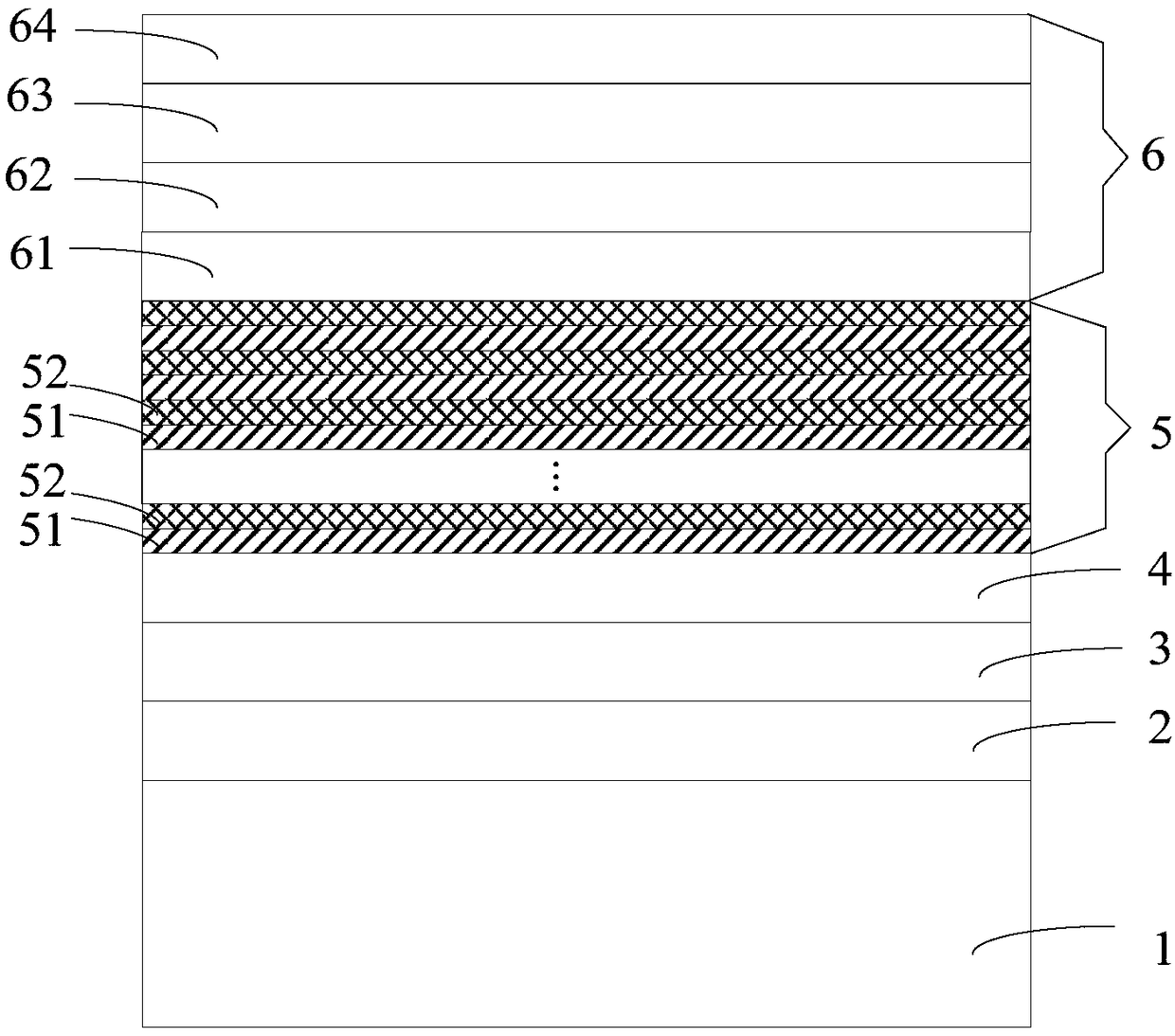
[0030] The invention provides a light emitting diode epitaxial wafer, figure 1 It is a schematic structural diagram of a light-emitting diode epitaxial wafer provided by an embodiment of the present invention, as shown in figure 1 As shown, the light-emitting diode epitaxial wafer includes a substrate 1 , and a buffer layer 2 , an undoped GaN layer 3 , an N-type layer 4 , an active layer 5 and a P-type layer 6 stacked on the substrate 1 in sequence. The active layer 5 includes B alternately grown in N periods x In 1.5x Ga 1-2.5x N well layer 51 and GaN barrier layer 52, 0x In 1.5x Ga 1-2.5x The thickness of the N well layer 51 is 4 to 20 nm.
[0031] In the embodiment of the present invention, by setting the active layer to include B alternately grown in N periods x In 1.5x Ga 1-2.5x N well layer and GaN barrier layer, 0x In 1.5x Ga 1-2.5x When the ratio of B component to In component in the N well layer is 2:3, it can make B x In 1.5x Ga 1-2.5x The final lattice ...
Embodiment 2
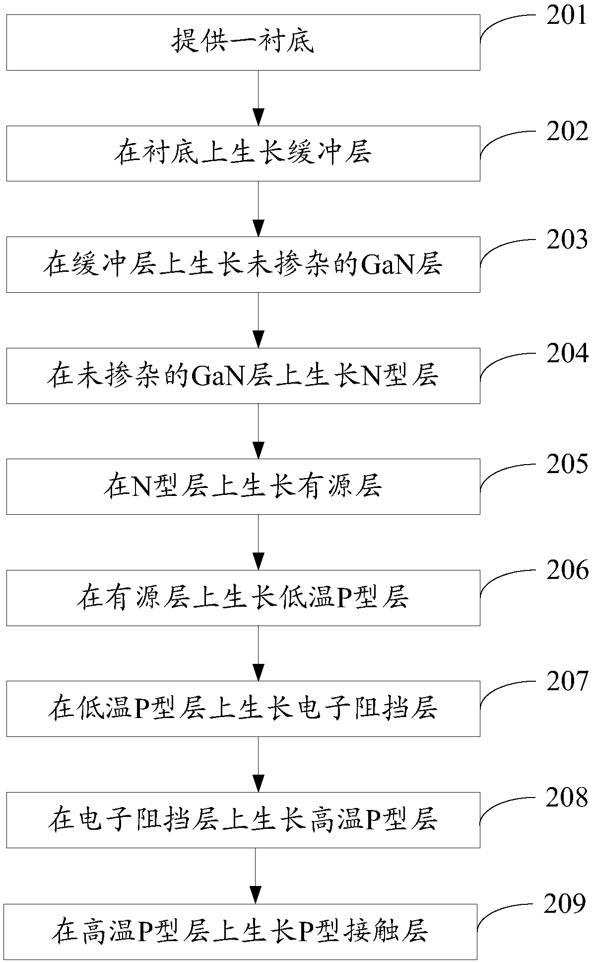
[0044] An embodiment of the present invention provides a method for manufacturing a light emitting diode epitaxial wafer, figure 2 It is a method flowchart of a method for manufacturing a light-emitting diode epitaxial wafer provided by an embodiment of the present invention, as shown in figure 2 As shown, the manufacturing method includes:
[0045] Step 201, providing a substrate.
[0046] Optionally, the substrate is a sapphire substrate.
[0047] In this embodiment, Veeco K465i or C4MOCVD (Metal Organic Chemical VaporDeposition, metal organic compound chemical vapor deposition) equipment is used to realize the LED growth method. Using high-purity H 2 (hydrogen) or high-purity N 2 (nitrogen) or high purity H 2 and high purity N 2 The mixed gas as the carrier gas, high-purity NH 3 As the N source, trimethylgallium (TMGa), triethylgallium (TEGa) and triethylboron (TEB) are used as the gallium source, trimethylindium (TMIn) is used as the indium source, and silane (SiH...
PUM
 Abstract
Description
Claims
Application Information