
Liquid crystal display panel

a liquid crystal display panel and liquid crystal technology, applied in non-linear optics, instruments, optics, etc., can solve the problems of uneven brightness by pressure, low-temperature bubble defects are display defects, uneven brightness, etc., to prevent low-temperature bubble defects and prevent uneven brightness

Active Publication Date: 2015-03-19
JAPAN DISPLAY INC
View PDF2 Cites 2 Cited by
  • Summary
  • Abstract
  • Description
  • Claims
  • Application Information

AI Technical Summary

Benefits of technology

The present invention relates to a method for forming multiple types of spacers differing in height using a multi-tone mask. By using a trapezoidal shape for each spacer and maintaining a ratio between top and bottom area of 0.3 or less, both low-temperature bubble defects and unevenness in brightness by pressure can be prevented without needing multiple types of spacers. Additionally, the invention achieves this while using spacers of a uniform height.

Problems solved by technology

However, low-temperature bubble defects and unevenness in brightness by pressure occur even in such liquid crystal display panels having the spacers between the transparent substrates, and thus countermeasures for preventing the low-temperature bubble defects and the unevenness in brightness by pressure are being requested.
The low-temperature bubble defects are display defects caused by vacuum bubbles (low-temperature bubbles) forming in the liquid crystal layer when the substrate distance cannot change smoothly following the volume contraction of the liquid crystal in a low-temperature environment.
The unevenness in brightness by pressure is a display defect occurring in regions of the liquid crystal display panel where the substrate distance has become nonuniform due to external pressure locally applied to a surface of a transparent substrate.

Method used


Image

  • Liquid crystal display panel
  • Liquid crystal display panel
  • Liquid crystal display panel

Examples


Embodiment Construction

[0027]Referring now to the drawings, a description will be given in detail of preferred embodiments of the present invention.

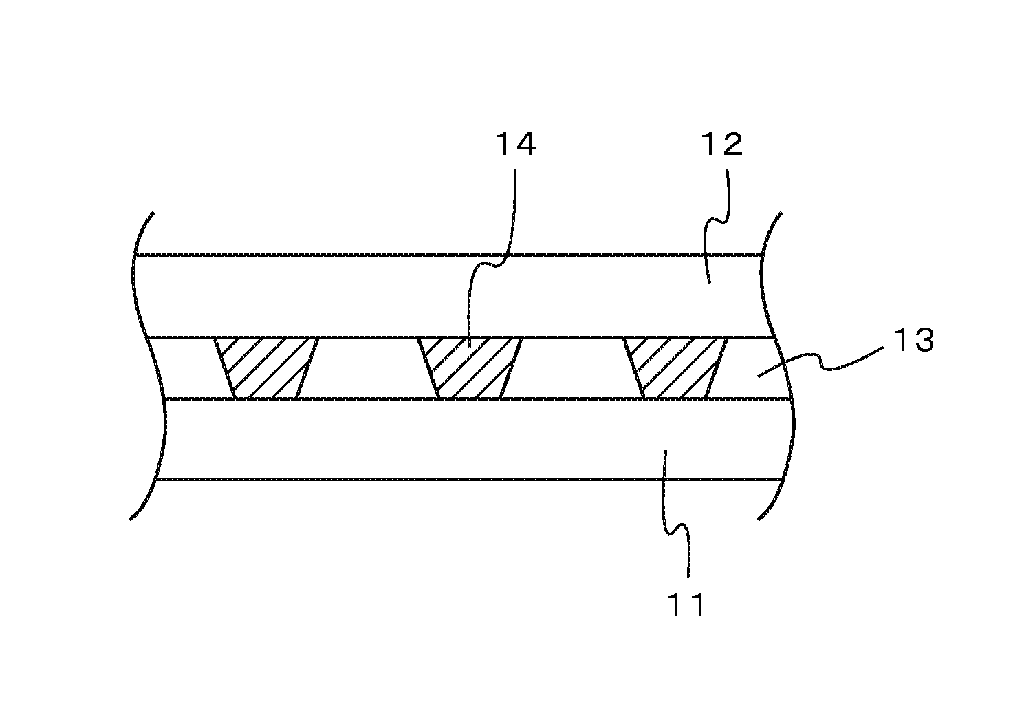
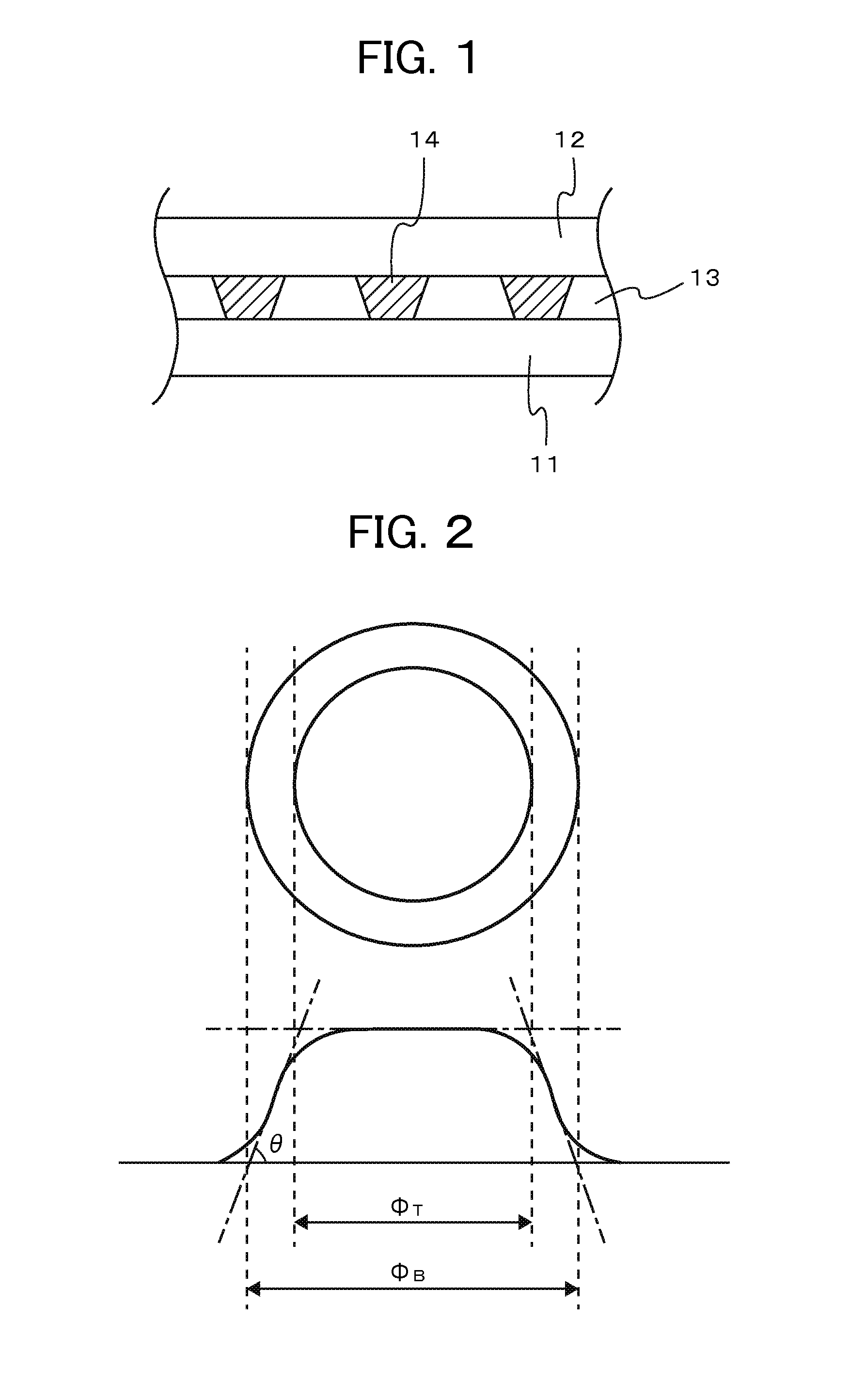
[0028]FIG. 1 is a vertical sectional view for explaining an embodiment of a liquid crystal display panel in accordance with the present invention. The liquid crystal display panel shown in FIG. 1 is characterized in that in a liquid crystal display panel comprising a plurality of spacers 14 arranged between a pair of transparent substrates 11 and 12 and a liquid crystal 13 encapsulated between the transparent substrates, the spacers 14 are of a uniform height and each spacer 14 is substantially in a trapezoidal shape in which the ratio between the top area and the bottom area is 0.3 or less.

[0029]The transparent substrates 11 and 12 are made of transparent material such as glass or resin. One of the transparent substrates 11 and 12 is used as an array substrate having a substrate surface on which an array of TFTs is arranged. The other substrate is used as a c...


PUM

PropertyMeasurementUnit
diameteraaaaaaaaaa
sizeaaaaaaaaaa
transmittanceaaaaaaaaaa

Abstract

Provided is a liquid crystal display panel in which both the prevention of low-temperature bubble defects and the prevention of unevenness in brightness by pressure can be achieved without the need of forming multiple types of spacers differing in the height. In a liquid crystal display panel comprising a plurality of spacers 14 arranged between a pair of transparent substrates 11 and 12 and a liquid crystal 13 encapsulated between the transparent substrates, the spacers 14 are of a uniform height and each spacer 14 is substantially in a trapezoidal shape in which the ratio between the top area and the bottom area is 0.3 or less. The spacers 14 are formed on one of the transparent substrates 11 and 12. The spacers 14 are arranged at appropriate density so that the contact area ratio of the spacers' top surfaces in contact with the opposing substrate per unit area is within a range of 0.8%-1.0%.

Description

CLAIM OF PRIORITY[0001]The present application claims priority from Japanese Patent Application JP 2013-192959 filed on Sep. 18, 2013, the content of which is hereby incorporated by reference into this application.BACKGROUND OF THE INVENTION[0002]1. Field of the Invention[0003]The present invention relates to a liquid crystal display panel, and in particular, to a liquid crystal display panel in which a liquid crystal gap is secured by arranging spacers between transparent substrates.[0004]2. Description of the Related Art[0005]Liquid crystal display panels (LCDs) are used as display devices of a variety of portable information devices such as cellular phones, personal digital assistants (PDAs), digital cameras and multimedia players.[0006]The liquid crystal display panel comprises a liquid crystal encapsulated between a pair of transparent substrates made of glass, resin or the like and performs the image display by driving and controlling the liquid crystal molecules by use of an ...

Claims


Application Information

Patent Timeline
Patent Type & Authority Applications(United States)
IPC IPC(8): G02F1/1339
CPCG02F1/13394G02F1/13398
Inventor ISHIGAKI, TOSHIMASASONODA, DAISUKEOTANI, MIHARUISHIBASHI, TSUTOMU
Owner JAPAN DISPLAY INC
Learn More