Touch panel

a touch panel and touch technology, applied in the field of touch panel, can solve the problems of inability to recognize the strength or force of the touch, degrade the visibility of the display, and complex structure, and achieve the effects of reducing thickness, improving touch pressure accuracy, and maximizing user experien

Active Publication Date: 2015-04-02
LG INNOTEK CO LTD
View PDF6 Cites 33 Cited by
  • Summary
  • Abstract
  • Description
  • Claims
  • Application Information

AI Technical Summary

Benefits of technology

[0007]The touch panel according to the embodiment includes a plurality of outer dummy layers with the piezoelectric material. The colors of the outer dummy layers may be variously implemented according to the piezoelectric material having the color.
[0008]The outer dummy layers can provide various tactile senses according to an intensity of touch pressure by pressure recognition. That is, the outer dummy layers can generate a piezoelectric effect.
[0009]Accordingly, the intensity and location of pressure can be deleted due to generation of a voltage at a touched point according to the touch pressure through the outer dummy layers.
[0010]Since a separate piezoelectric layer for providing a vibrating force may be omitted due to the outer dummy layers, thickness reduction may be achieved. Further, a user's experience can be maximized by implementing the feedback through the touch pressure. That is, the accuracy of the touch pressure can be improved by implementing tactile sense feedback on a touch panel through the outer dummy layers, and the user's experience can be maximized by providing the feeling of textures. In detail, roughness or softness of an object displayed on a display can be provided.
[0011]Further, a plurality of outer dummy layers are provided so that a tactile sense may be impressed to a plurality of partial areas. Mutually different tactile sense feedbacks can be generated from a plurality of partial areas XL, XR, YL, and YR. Accordingly, various tactile senses can be represented due to overlap vibration of four surfaces of up, down, left and right surfaces. In addition, beats can be induced to a surface where tactile senses are generated due to the interaction of partial vibrations, and various types of vibration patterns may be generated.
[0012]In addition, when an input tool such as a finger touches a top surface of the substrate, a voltage and an excitation frequency vary, and the outer dummy layer generates an ultrasonic wave so that the substrate may vibrate. Pressure of an air layer between the finger and the substrate may vary due to the vibration of the substrate. In addition, a viscosity of the air layer may vary to generate a tactile sense, and a unique tactile sense can be provided. That is, when touched, a tactile sense caused by variations in the viscosity and pressure property of the air layer may be provided by adjusting excitation frequency characteristics.

Problems solved by technology

A resistive type touch panel and a capacitive type touch panel according to the related art may simply recognize only location information of a touch but cannot recognize strength or force of the touch when all screen inputs are achieved.
In addition, since a touch panel layer is placed at a top end of a display layer, a structure becomes complicated and the visibility of a display is degraded.
However, as the electronic appliances have been extensively used, there are various demands of users to use the electronic appliances having various functions.

Method used


Image

  • Touch panel
  • Touch panel
  • Touch panel

Examples


first embodiment

[0024]First, a touch panel will be described in detail with reference to FIGS. 1 to 6.

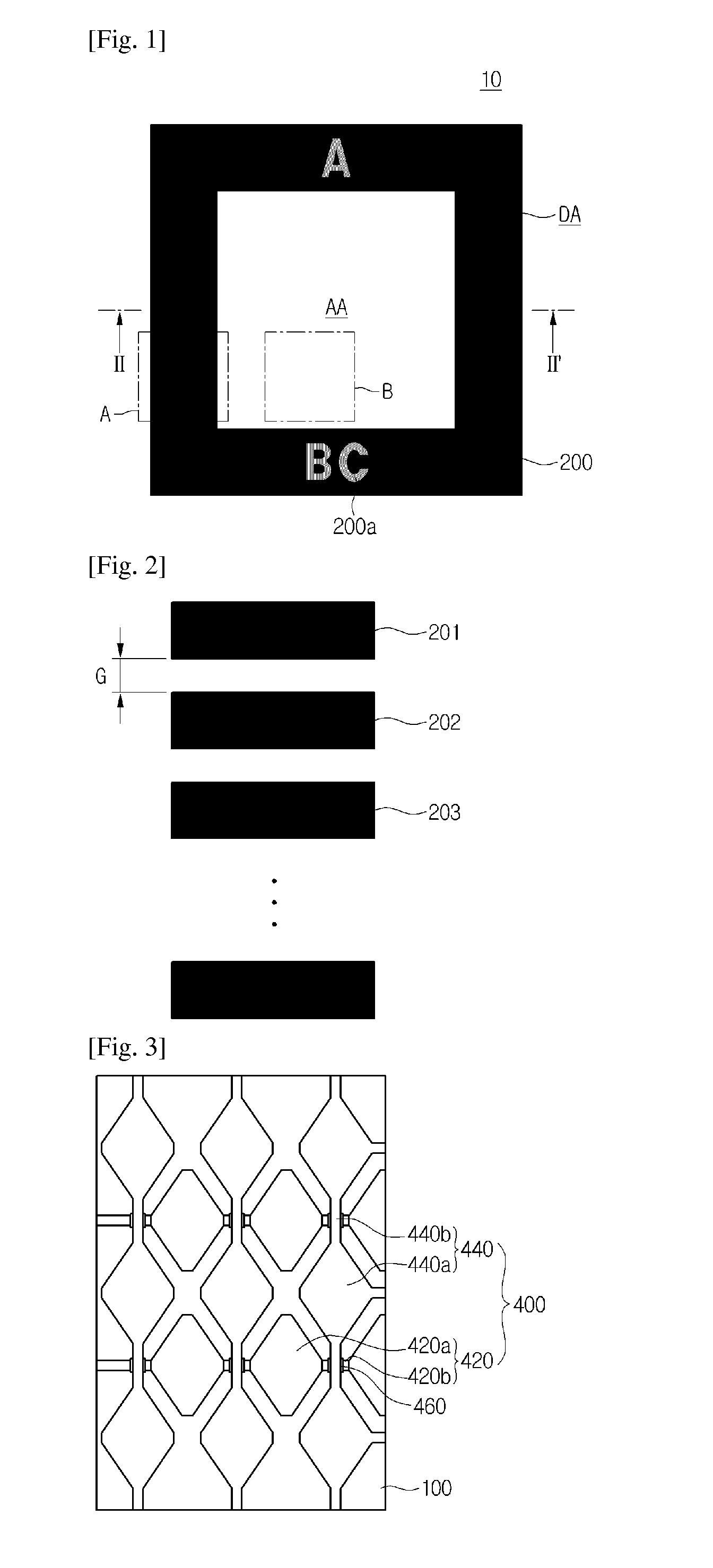
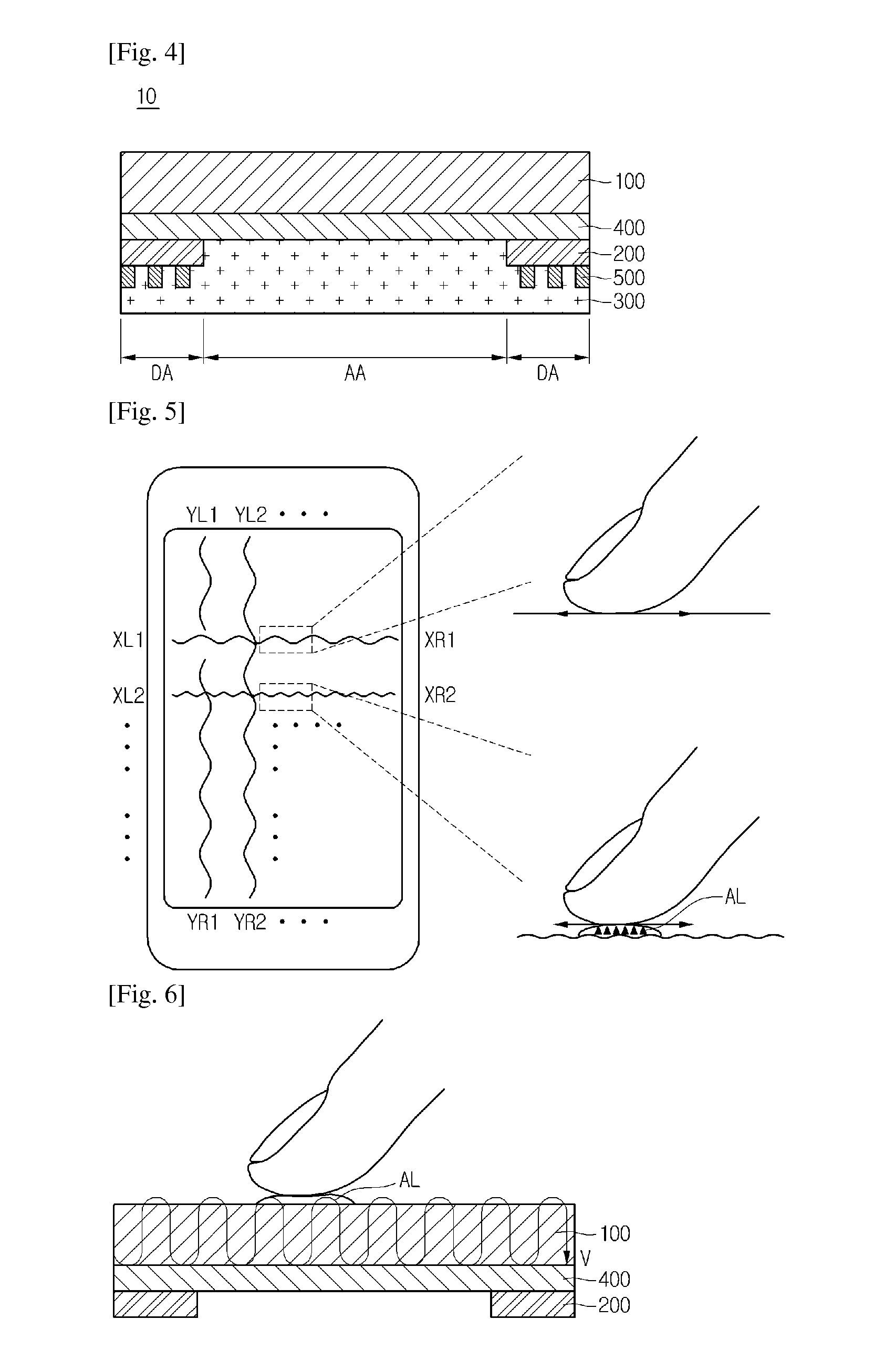
[0025]FIG. 1 is a schematic plan view showing a touch panel according to the first embodiment. FIG. 2 is an enlarged plan view of an ‘A’ portion of FIG. 1. FIG. 2 is an enlarged plan view of a ‘B’ portion of FIG. 1. FIG. 2 is a sectional view taken along line II-II′of FIG. 1. FIGS. 5 and 6 are views illustrating driving of the touch panel according to the embodiment.

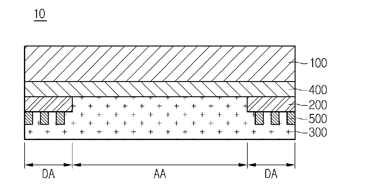
[0026]Referring to FIGS. and 4, the touch panel 10 according to the first embodiment includes an effective area AA for detecting apposition of an input device and a dummy area DA disposed around the effective area AA.

[0027]A transparent electrode 400 for detecting the input device may be formed on the effective area AA. In addition, a wire 500 connected to the transparent electrode 400 and a printed circuit board (not shown) connecting the wire 500 to an external circuit (not shown) may be formed on the dummy area DA. An outer dummy la...

second embodiment

[0064]FIG. 7 is a sectional view showing a touch panel according to a

[0065]In the touch panel 20 according to the second embodiment, an outer dummy layer 220 may be placed between a transparent electrode 420 and a substrate 100. That is, the outer dummy layer 220 may be placed on the substrate 100, and the transparent electrode 420 may be placed on the outer dummy layer 220 and the substrate 100. Accordingly, various structures of the touch panel can be ensured.

[0066]Any reference in this specification to “one embodiment,”“an embodiment,”“example embodiment,” etc., means that a particular feature, structure, or characteristic described in connection with the embodiment is included in at least one embodiment of the invention. The appearances of such phrases in various places in the specification are not necessarily all referring to the same embodiment. Further, when a particular feature, structure, or characteristic is described in connection with any embodiment, it is submitted that...


PUM


Abstract

A touch panel according to the embodiment includes a substrate including an effective area and a dummy area surrounding the effective area; a transparent electrode on the substrate; and an outer dummy layer on the dummy area, wherein the outer dummy layer comprises a piezoelectric material.

Description

TECHNICAL FIELD[0001]The disclosure relates to a touch panel.BACKGROUND ART[0002]A resistive type touch panel and a capacitive type touch panel according to the related art may simply recognize only location information of a touch but cannot recognize strength or force of the touch when all screen inputs are achieved. In addition, since a touch panel layer is placed at a top end of a display layer, a structure becomes complicated and the visibility of a display is degraded. Accordingly, researches and studies have been performed toward a touch panel using a piezoelectric element other than an existing scheme.[0003]Since the piezoelectric element has a property capable of converting a mechanical signal such as pressure into an electric signal, the piezoelectric element has been extensively used for a sensor such as a pressure sensor or an ultrasonic sensor.[0004]However, as the electronic appliances have been extensively used, there are various demands of users to use the electronic ...

Claims


Application Information

Patent Timeline
Patent Type & Authority Applications(United States)
IPC IPC(8): H03K17/96G06F3/041
CPCH03K17/9622G06F3/0414H03K2217/960755H03K2217/960745H03K2217/96062G06F3/0446G06F3/0443G06F3/04142H10N30/206H10N30/857G02F1/13338G06F3/0444G06F3/044
Inventor LEEYUN, JI SUNCHAI, KYOUNG HOON
Owner LG INNOTEK CO LTD
Why Eureka
Try Eureka