Check patentability & draft patents in minutes with Patsnap Eureka AI!

Multi-die stack structure

a stack structure and die technology, applied in the direction of semiconductor devices, semiconductor/solid-state device details, instruments, etc., can solve the problem of large input-output capacitance difference between cs/zq pads and ladder-style connections in ddr3 sdrams, and achieve the effect of reducing the input capacitance differen

Active Publication Date: 2015-04-09
NAN YA TECH
View PDF3 Cites 0 Cited by
  • Summary
  • Abstract
  • Description
  • Claims
  • Application Information

AI Technical Summary

Benefits of technology

This patent describes a way to reduce the difference in input capacitance between different dies in a multi-die stack structure. This is achieved by connecting specific pads on the bottom die with specific pads on the overlying dies. This reduces the variation in external input signals and ensures consistent timing and calibration results between different dies.

Problems solved by technology

However, the ladder-style connection in DDR3 SDRAM suffers from large input-capacitance (Cin) difference between the CS / ZQ pads.

Method used


Image

  • Multi-die stack structure
  • Multi-die stack structure

Examples


Embodiment Construction

[0016]This invention will be further explained with an embodiment, which is however not intended to restrict the scope of this invention. For example, though N is equal to 4 in the embodiment, N may alternatively be less or more than 4, such as 2 or 8.

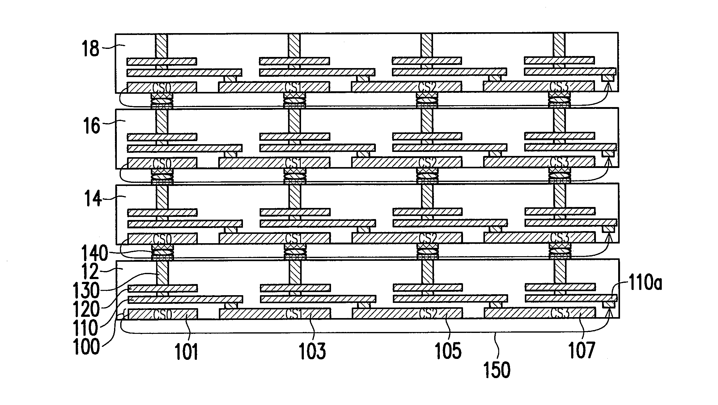
[0017]FIG. 2 illustrates a multi-die stack structure of QDP type according to an embodiment of this invention, which has a ladder-style connection between the dies that is based on CS (Chip-Select) pads.

[0018]In each of the dies 12, 14, 16 and 18, the metal layer 110 having been defined into the CS0 pad 101, the CS1 pad 103, the CS2 pad 105, the CS3 pad 107 and the other pads (not shown, including ZQ pads and so on) may be the third metal (M3) layer of the die 12, 14, 16 or 18.

[0019]The ladder-style connection is described in details below.

[0020]In the 2nd die 14, the CS0 pad 101 as the specific die for the input of the 2nd die 14 is electrically connected with the CS1 pad 103 of the 1st die 12 via a solder ball 140, a TSV 130 in the 1...


PUM


Abstract

A multi-die stack structure including N dies stacked vertically is described. N is an integer larger than or equal to 2. Each die includes N die-specific input pads, wherein a specific pad among the N pads is for the input of the die. The specific pad of each die above the bottom die is electrically connected with a different pad of the bottom die other than the specific pad of the bottom die, via at least one TSV and, when not being in the die neighboring to the bottom die, also via a different pad of each underlying die above the bottom die. The specific pad of the bottom die is electrically connected with at least one pad of the overlying die(s) that is not the specific pad of any overlying die and not any pad electrically connected with the specific pad of any overlying die.

Description

BACKGROUND[0001]1. Field of the Invention[0002]The invention relates to an integrated circuit structure, and particularly relates to a multi-die stack structure.[0003]2. Description of Related Art[0004]Multi-die stack structures are often applied to electronic products that require increased memory density and / or device performance in a reduced package size.[0005]FIG. 1 illustrates a conventional multi-die stack structure of QDP (quad-die package) type with a “ladder-style” connection between the dies that is based on CS (Chip-Select) pads. Such a structure is currently applied to DDR3 SDRAM (Double-Data-Rate Three Synchronous Dynamic Random Access Memory).[0006]Referring to FIG. 1, the structure includes four dies 12, 14, 16 and 18 vertically stacked from bottom to top. Each die 12, 14, 16 or 18 has four CS pads including a CS0 pad 101 for the input of the die, a CS1 pad 103 for the input of the 1-level higher die (if present), a CS2 pad 105 for the input of the 2-level higher die ...

Claims


Application Information

Patent Timeline
Patent Type & Authority Applications(United States)
IPC IPC(8): H01L23/00H01L25/065H01L23/538
CPCH01L24/14H01L23/5384H01L2225/06544H01L2224/1405H01L25/0657H01L2225/06527H01L2225/06513H01L24/05H01L2224/16146G11C5/063H01L23/522G11C2029/0403H01L2224/0401H01L2224/1134
Inventor LIANG, ZERSUZUKI, KOTARO
Owner NAN YA TECH
Features
  • R&D
  • Intellectual Property
  • Life Sciences
  • Materials
  • Tech Scout
  • Unparalleled Data Quality
  • Higher Quality Content
  • 60% Fewer Hallucinations
Learn More