Thinning in package using separation structure as stop

Active Publication Date: 2015-04-23
INFINEON TECH AG
View PDF9 Cites 99 Cited by
  • Summary
  • Abstract
  • Description
  • Claims
  • Application Information

AI Technical Summary

Benefits of technology

[0005]There may be a need to perform thinning of electronic chips or wafers with high accuracy and

Problems solved by technology

However, accurately thinning wafers electronic chips and handling

Method used


Image

  • Thinning in package using separation structure as stop
  • Thinning in package using separation structure as stop
  • Thinning in package using separation structure as stop

Examples


Embodiment Construction

[0012]In the following, further exemplary embodiments of the methods, and the encapsulated chip structure will be explained.

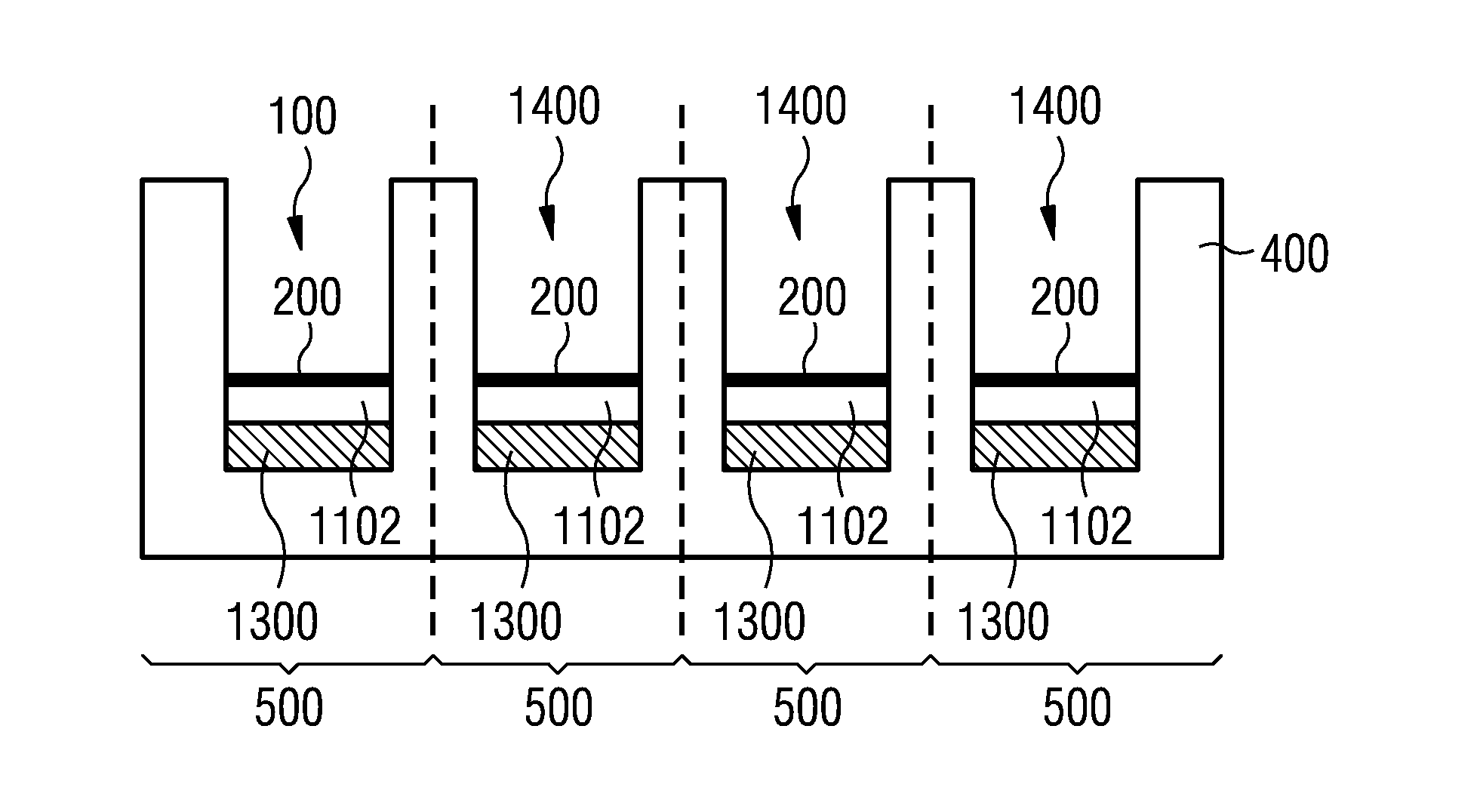
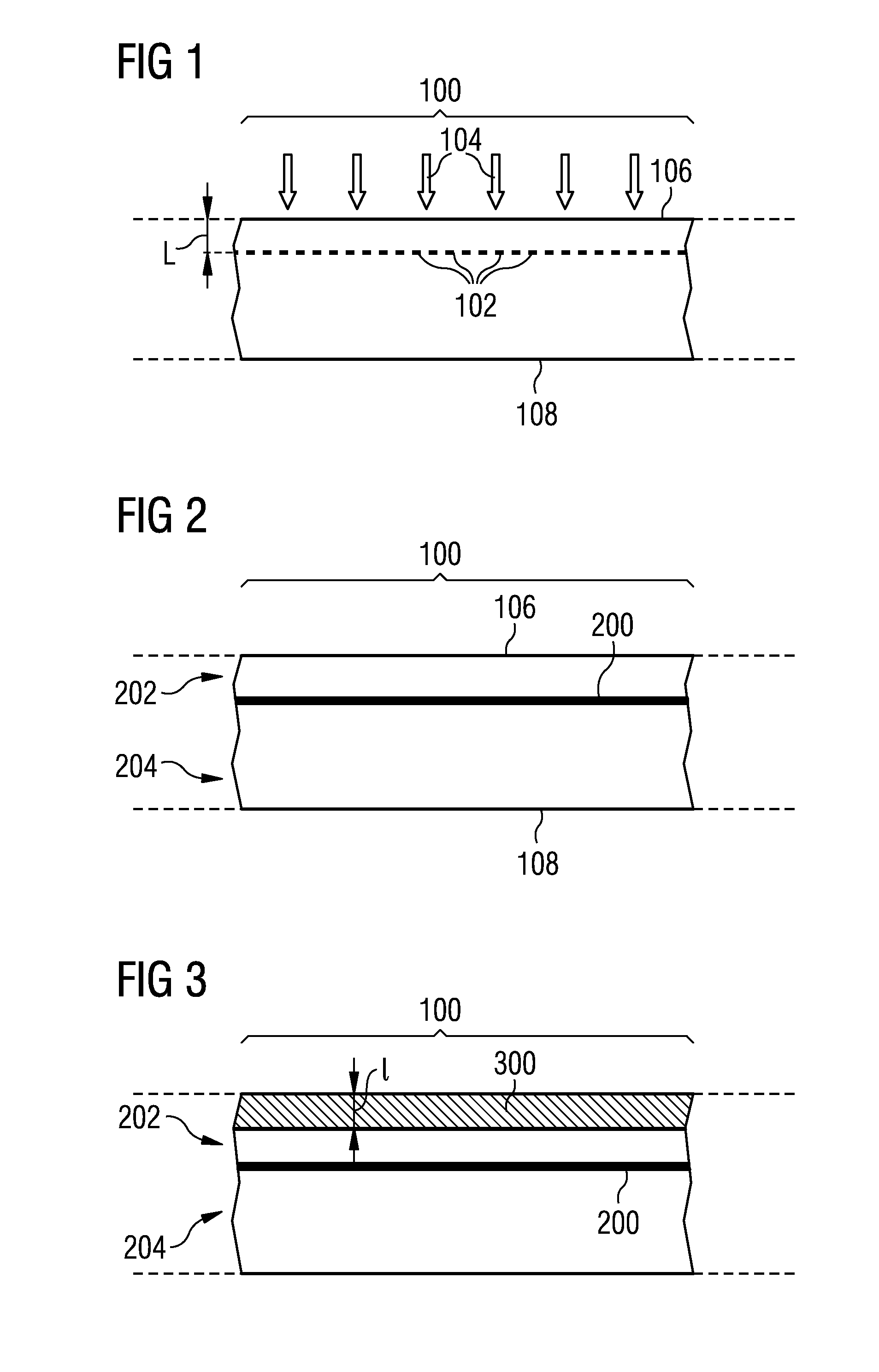
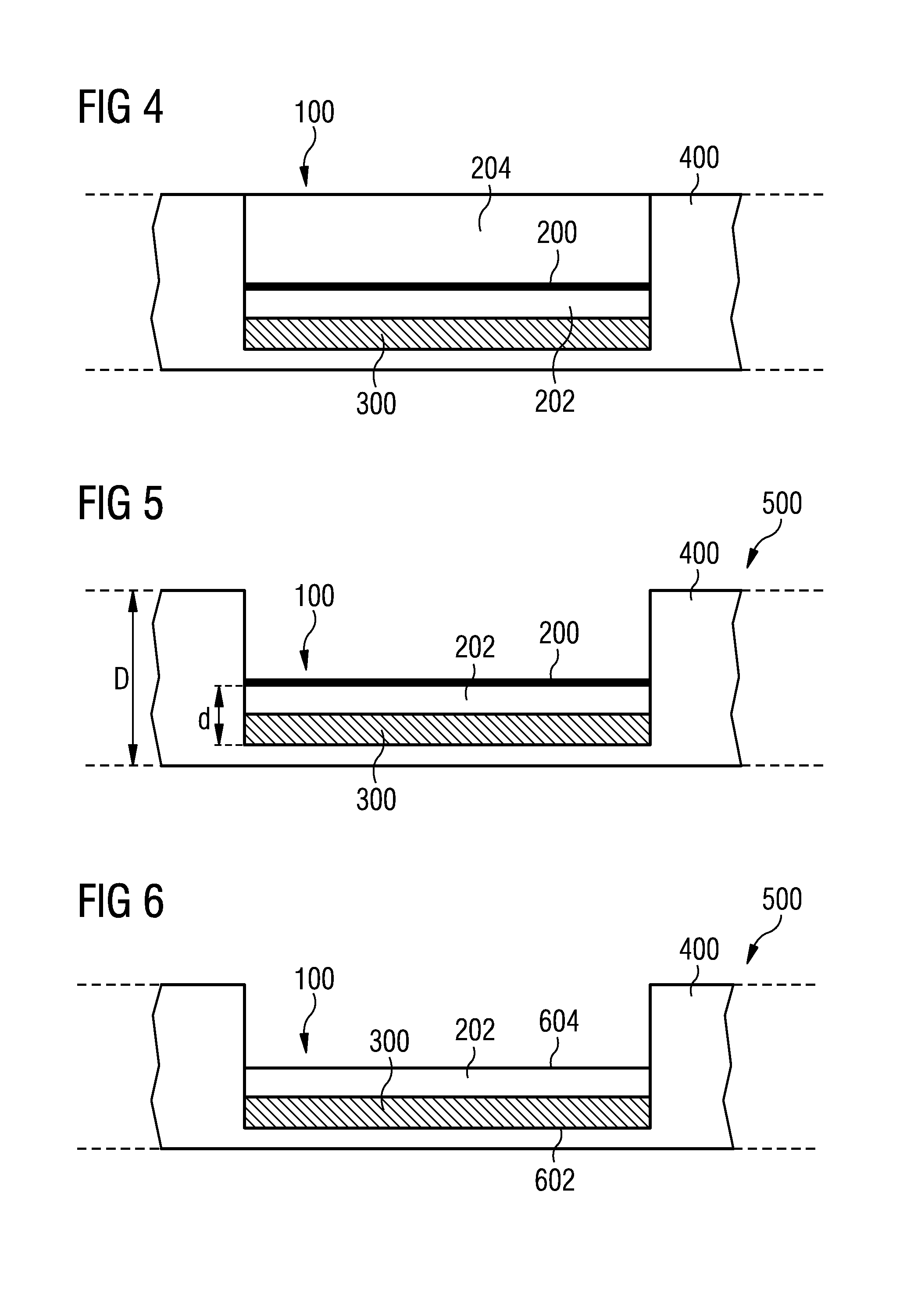
[0013]In the context of the present application, the term “encapsulated chip structure” may particularly denote a structure having one or more electronic chips (such as a semiconductor chip being singularised from a wafer or still forming part of a wafer) which is mounted within an encapsulating structure (such as a mold structure) as package. Such an electronic chip may have a thickness smaller than a thickness of a standard wafer and / or smaller than a thickness of the encapsulating structure.

[0014]In the context of the present application, the term “separation structure” may particularly denote a structure embedded in an interior of an electronic chip which locally has different chemical and / or physical properties, in particular in terms of its etchability (i.e. its capability of being etched), as compared to neighboring material. In particular, the material ...


PUM


Abstract

A method of forming a thinned encapsulated chip structure, wherein the method comprises providing a separation structure arranged within an electronic chip, encapsulating part of the electronic chip by an encapsulating structure, and thinning selectively the electronic chip partially encapsulated by the encapsulating structure so that the encapsulating structure remains with a larger thickness than the thinned electronic chip, wherein the separation structure functions as a thinning stop.

Description

BACKGROUND[0001]1. Field[0002]The present invention relates to a method of forming a thinned encapsulated chip structure, a method of forming a thinned encapsulated semiconductor device, a method of forming thinned encapsulated electronic chips, and an encapsulated chip structure.[0003]2. Description of the Related Art[0004]In many technological fields, electronic chips encapsulated within an encapsulating structure are used. There is a continuing trend to provide the electronic chips with a very small thickness, for instance for power applications. However, accurately thinning wafers electronic chips and handling them for encapsulating and subsequent processing is a challenge.SUMMARY[0005]There may be a need to perform thinning of electronic chips or wafers with high accuracy and without the risk of quality deteriorations during handling of thinned electronic chips or wafers.[0006]According to an exemplary embodiment, a method of forming a thinned encapsulated chip structure is pro...

Claims


Application Information

Patent Timeline
IPC IPC(8): H01L23/28H01L21/56
CPCH01L23/28H01L21/561H01L21/56H01L23/13H01L23/31H01L2924/0002H01L2924/00H01L21/76254H01L23/3128H01L23/3185H01L24/96H01L2224/04105H01L2224/12105H01L21/76251H01L21/76259H01L21/78
Inventor ENGELHARDT, MANFREDFUERGUT, EDWARDEDER, HANNES
Owner INFINEON TECH AG
Why Eureka
Try Eureka