Interposer and method for manufacturing same

a technology of interposer and manufacturing method, which is applied in the direction of dielectric characteristics, printed element electric connection formation, printed circuit aspects, etc., can solve the problems of time-consuming and complex process

Active Publication Date: 2015-05-21
LEADING INTERCONNECT SEMICON TECH QINHUANGDAO CO LTD +1
View PDF1 Cites 0 Cited by
  • Summary
  • Abstract
  • Description
  • Claims
  • Application Information

AI Technical Summary

Problems solved by technology

However, the process is complex and time-consuming.

Method used


Image

  • Interposer and method for manufacturing same
  • Interposer and method for manufacturing same
  • Interposer and method for manufacturing same

Examples


Embodiment Construction

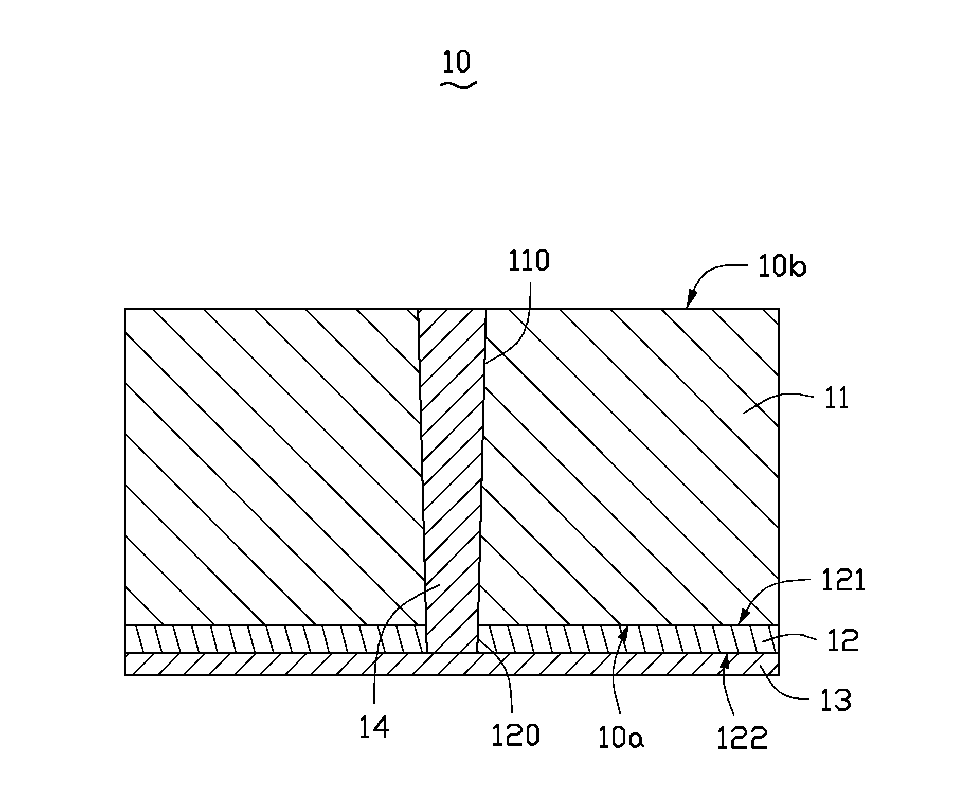
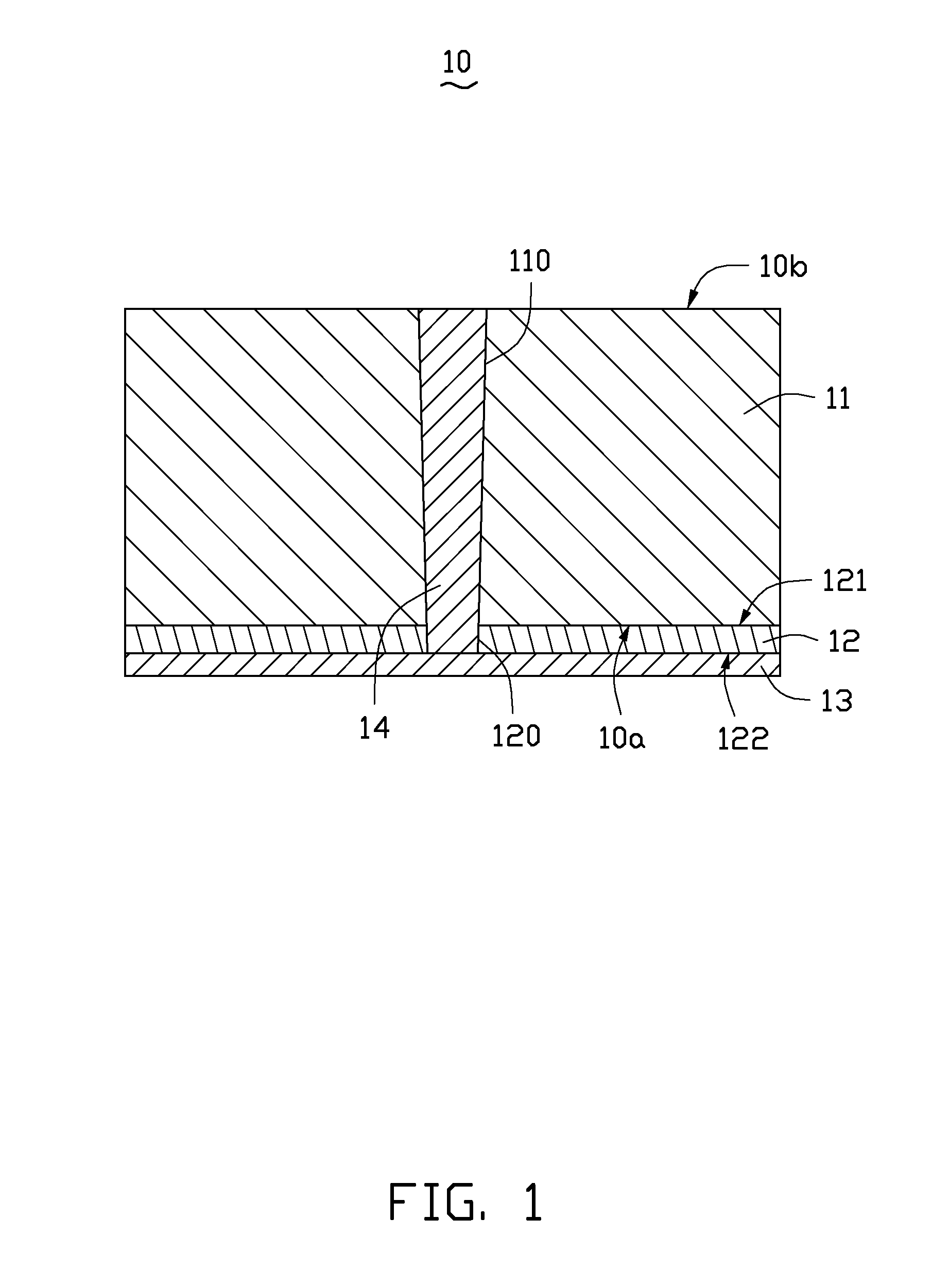
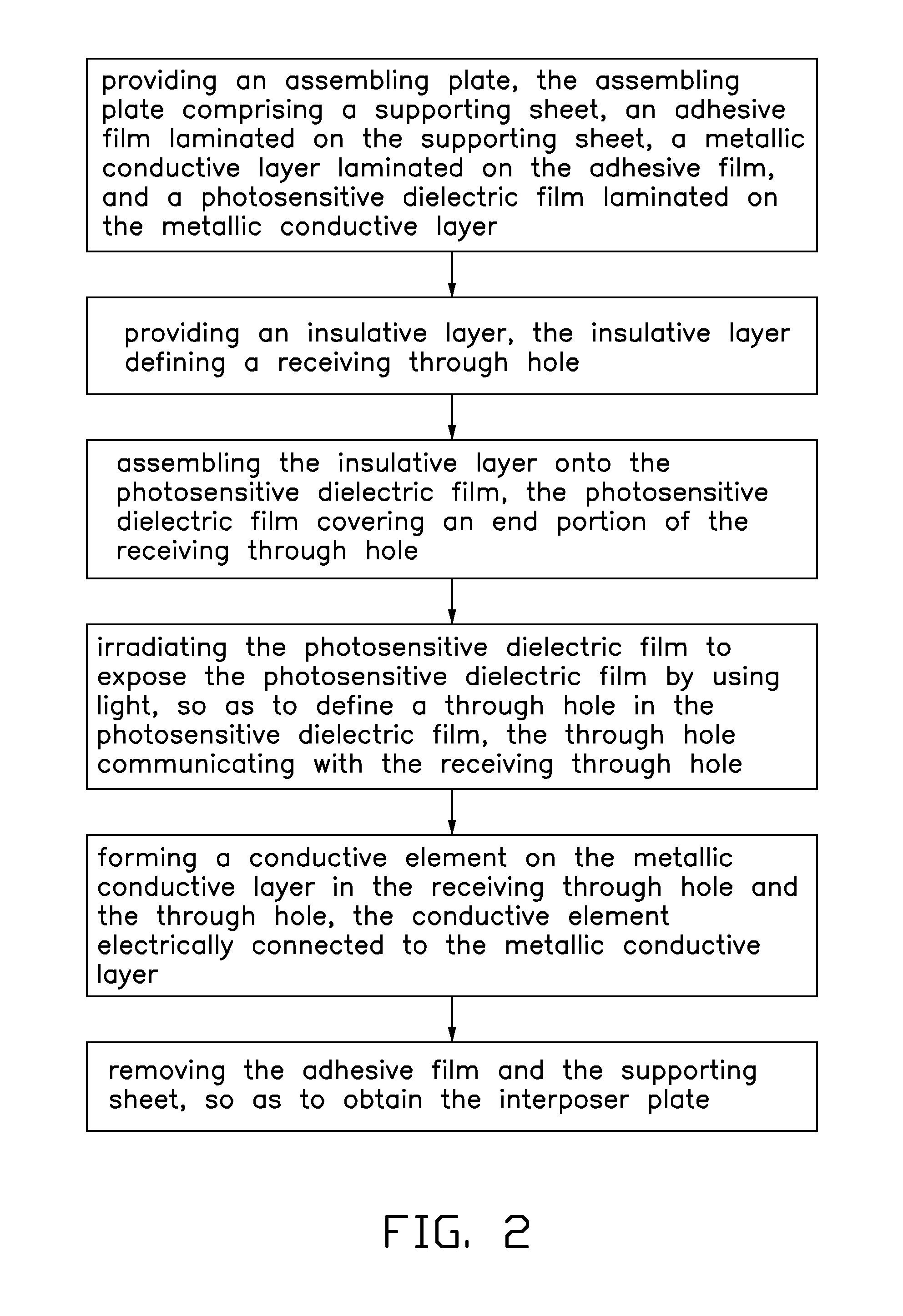
[0010]FIG. 1 shows an embodiment of an interpose plate 10. The interpose plate 10 includes an insulating substrate 11, a photosensitive dielectric film 12, a conductive layer 13, and a conductive via 14.

[0011]The insulating substrate 11 includes a bottom surface 10a and a top surface 10b. The bottom surface 10a is substantially parallel to the top surface 10b. In one embodiment, the insulating substrate 11 is made of glass. The insulating substrate 11 defines a receiving through hole 110 extending through the bottom surface 10a and the top surface 10b.

[0012]The photosensitive dielectric film 12 is mounted on the bottom surface 10a. In one embodiment, the photosensitive dielectric film 12 is made of photosensitive polyimides. The photosensitive dielectric film 12 includes a supporting surface 121 contacting the bottom surface 10a and a lower surface 122 facing away from the bottom surface 10a. The photosensitive dielectric film 12 defines a through hole 120 spatially corresponding t...


PUM

PropertyMeasurementUnit
photosensitiveaaaaaaaaaa
conductiveaaaaaaaaaa
insulatingaaaaaaaaaa

Abstract

An interposer includes an insulating substrate, a photosensitive dielectric film, a conductive layer, and a conductive via. The insulating substrate includes a bottom surface and a top surface, and defines a receiving through hole extending through the bottom surface and the top surface. The photosensitive dielectric film is mounted on the bottom surface. The photosensitive dielectric film defines a through hole spatially corresponding to and communicating with the receiving through hole. The conductive layer is mounted on an end of the photosensitive dielectric film away from the insulating substrate. The conductive layer covers an end of the through hole.The conductive via is received in the receiving through hole and the through hole. The conductive via contacts and electrically connects to the conductive layer.

Description

BACKGROUND[0001]1. Technical Field[0002]The present disclosure relates to an interposer and a method for manufacturing the interposer.[0003]2. Description of Related Art[0004]Manufacturing processes of interposers includes forming a seed layer in a receiving through hole of an insulating substrate. However, the process is complex and time-consuming. Furthermore, the seed layer generates thermal stress on the interposer.[0005]Therefore, what is needed is an interposer and a method for manufacturing the interposer that can overcome the above-mentioned limitations.BRIEF DESCRIPTION OF THE DRAWINGS[0006]Many aspects of the present embodiments can be better understood with reference to the following drawings. The components in the drawings are not necessarily drawn to scale, the emphasis instead being placed upon clearly illustrating the principles of the present embodiments. Moreover, in the drawings, all the views are schematic, and like reference numerals designate corresponding parts...

Claims


Application Information

Patent Timeline
Patent Type & Authority Applications(United States)
IPC IPC(8): H05K1/11H05K3/40H05K1/03
CPCH05K1/115H05K1/0306H05K2201/0959H05K2201/0104H05K3/4038H05K3/423H05K3/007H05K3/421H05K3/427Y10T29/49165
Inventor LEE, TAEKOO
Owner LEADING INTERCONNECT SEMICON TECH QINHUANGDAO CO LTD
Why Eureka
Try Eureka