
Discrete semiconductor device package and manufacturing method

a semiconductor device and manufacturing method technology, applied in the field of semiconductor device packages, can solve the problems of cumbersome and time-consuming wire bonding, inability to manufacture an approach to reproduce the small dimensions of a discrete semiconductor device at the package level in a straightforward and cost-effective manner, and inability to meet the requirements of discrete semiconductor device dimensions,

Active Publication Date: 2015-05-21
NEXPERIA BV
View PDF2 Cites 1 Cited by
  • Summary
  • Abstract
  • Description
  • Claims
  • Application Information

AI Technical Summary

Benefits of technology

Enables cost-effective and efficient miniaturization of semiconductor packages by avoiding wire bonds, facilitating smaller package sizes and improved robustness through solder-based connections, and allowing for batch manufacturing processes.

Problems solved by technology

In the known packaging approaches, the package contacts are typically fan-outs of the contacts of the discrete semiconductor device, i.e. have a larger area, as manufacturing approaches to reproduce the small dimensions of a discrete semiconductor device at the package level in a straightforward and cost-effective manner are currently unavailable.
For instance, for diode packages, it is difficult to miniaturize the package beyond dimensions of 0.6 mm×0.3 mm×0.3 mm.
However, miniaturization beyond the dimensions of the 0603 packages makes it cumbersome and time-consuming to apply wire bonds, thus making the use of such connections practically unfeasible.

Method used


Image

  • Discrete semiconductor device package and manufacturing method
  • Discrete semiconductor device package and manufacturing method
  • Discrete semiconductor device package and manufacturing method

Examples


Embodiment Construction

[0022]Embodiments of the invention are described in more detail and by way of non-limiting examples with reference to the accompanying drawings, wherein:

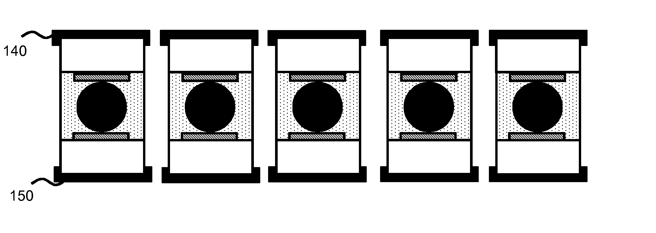
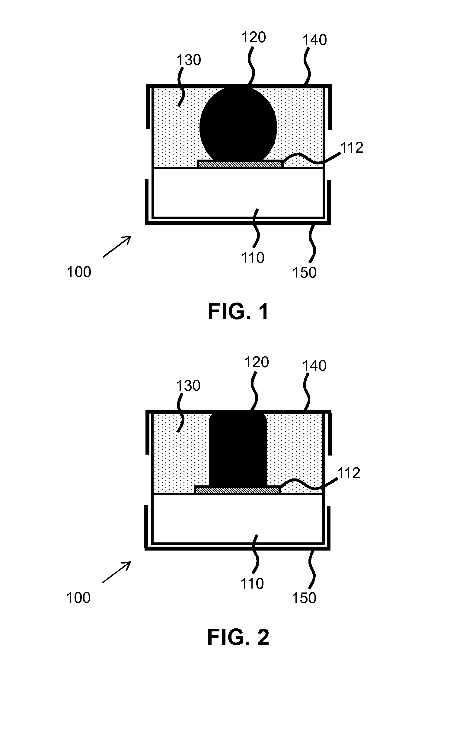
[0023]FIG. 1 schematically depicts a discrete semiconductor device package according to an embodiment of the present invention;

[0024]FIG. 2 schematically depicts a discrete semiconductor device package according to another embodiment of the present invention;

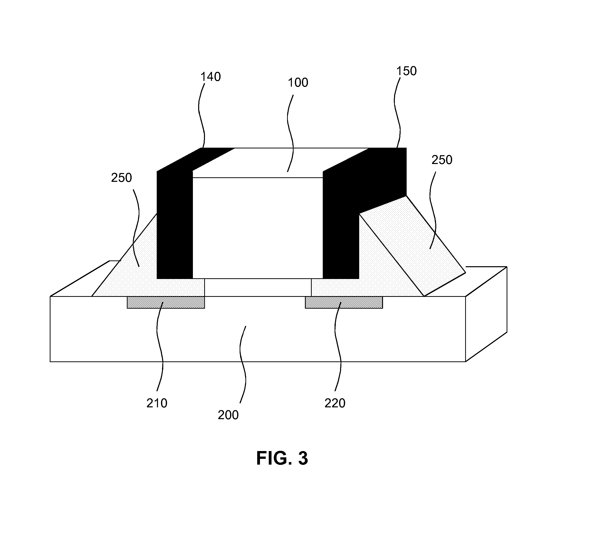
[0025]FIG. 3 schematically depicts a carrier including a discrete semiconductor device package according to an embodiment of the present invention;

[0026]FIG. 4 schematically depicts the various steps of a method of manufacturing a discrete semiconductor device package according to an embodiment of the present invention;

[0027]FIG. 5 schematically depicts the various steps of a method of manufacturing a discrete semiconductor device package according to another embodiment of the present invention; and

[0028]FIG. 6 schematically depicts the various steps of a method of manufacturing...


PUM


Abstract

Disclosed is a discrete semiconductor device package (100) comprising a semiconductor die (110) having a first surface and a second surface opposite said first surface carrying a contact (112); a conductive body (120) on said contact; an encapsulation material (130) laterally encapsulating said conductive body; and a capping member (140, 610) such as a solder cap, a further semiconductor die or a combination thereof in conductive contact with the solder portion, said solder cap extending over the encapsulation material. A further solder cap (150) may be provided over the first surface. A method of manufacturing such a discrete semiconductor device package is also disclosed.

Description

FIELD OF THE INVENTION[0001]The present invention relates to a discrete semiconductor device package. The present invention further relates to a method of packaging a discrete semiconductor device such as a diode.BACKGROUND OF THE INVENTION[0002]Discrete semiconductor devices such as diodes are typically provided in a package when marketed. The package protects the discrete semiconductor device from accidental damage and provides the contacts for integrating the discrete semiconductor device in a larger electronic device, e.g. by mounting the discrete semiconductor device on a carrier such as a printer circuit board (PCB). In the known packaging approaches, the package contacts are typically fan-outs of the contacts of the discrete semiconductor device, i.e. have a larger area, as manufacturing approaches to reproduce the small dimensions of a discrete semiconductor device at the package level in a straightforward and cost-effective manner are currently unavailable.[0003]As a conseq...

Claims


Application Information

Patent Timeline
Patent Type & Authority Applications(United States)
IPC IPC(8): H01L21/78H01L21/56
CPCH01L21/56H01L21/78H01L2224/051H01L2224/05088H01L2224/20H01L24/03H01L24/05H01L24/06H01L24/13H01L24/16H01L24/81H01L25/0657H01L2224/04105H01L2224/05016H01L2224/06181H01L2224/94H01L2924/10253H01L2224/32113H01L2224/32105H01L24/29H01L24/32H01L24/33H01L2224/0346H01L2224/04026H01L2224/05111H01L2224/05147H01L2224/05573H01L2224/05582H01L2224/05611H01L2224/05639H01L2224/05644H01L2224/13147H01L2224/291H01L2224/33181H01L2224/9202H01L2224/96H01L2224/05568H01L25/50H01L2225/06513H01L2225/06565H01L2224/16145H01L2224/32237H01L2924/00014H01L2224/0401H01L2924/12036H01L2924/014H01L2924/00H01L2224/03H01L2224/81H01L2224/05552H01L24/11H01L24/12
Inventor BOETTCHER, TIMWALCZYK, SVENGROENHUIS, ROELF ANCO JACOBBRENNER, ROLFDE BRUIN, EMIEL
Owner NEXPERIA BV
Features
  • Generate Ideas
  • Intellectual Property
  • Life Sciences
  • Materials
  • Tech Scout
  • Unparalleled Data Quality
  • Higher Quality Content
  • 60% Fewer Hallucinations
Learn More