Method for producing light-emitting diode
a technology of light-emitting diodes and diodes, which is applied in the direction of semiconductor/solid-state device manufacturing, electrical apparatus, semiconductor devices, etc., can solve the problems of insufficient transmission of heat generated by light-emitting chips to the carrier, inability to control the quantity of glue and the area of die-bonding adhesive layers, and inability to absorb light-emitting chips
- Summary
- Abstract
- Description
- Claims
- Application Information
AI Technical Summary
Benefits of technology
Problems solved by technology
Method used
Image

Examples
first embodiment
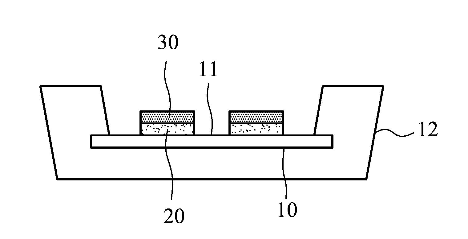
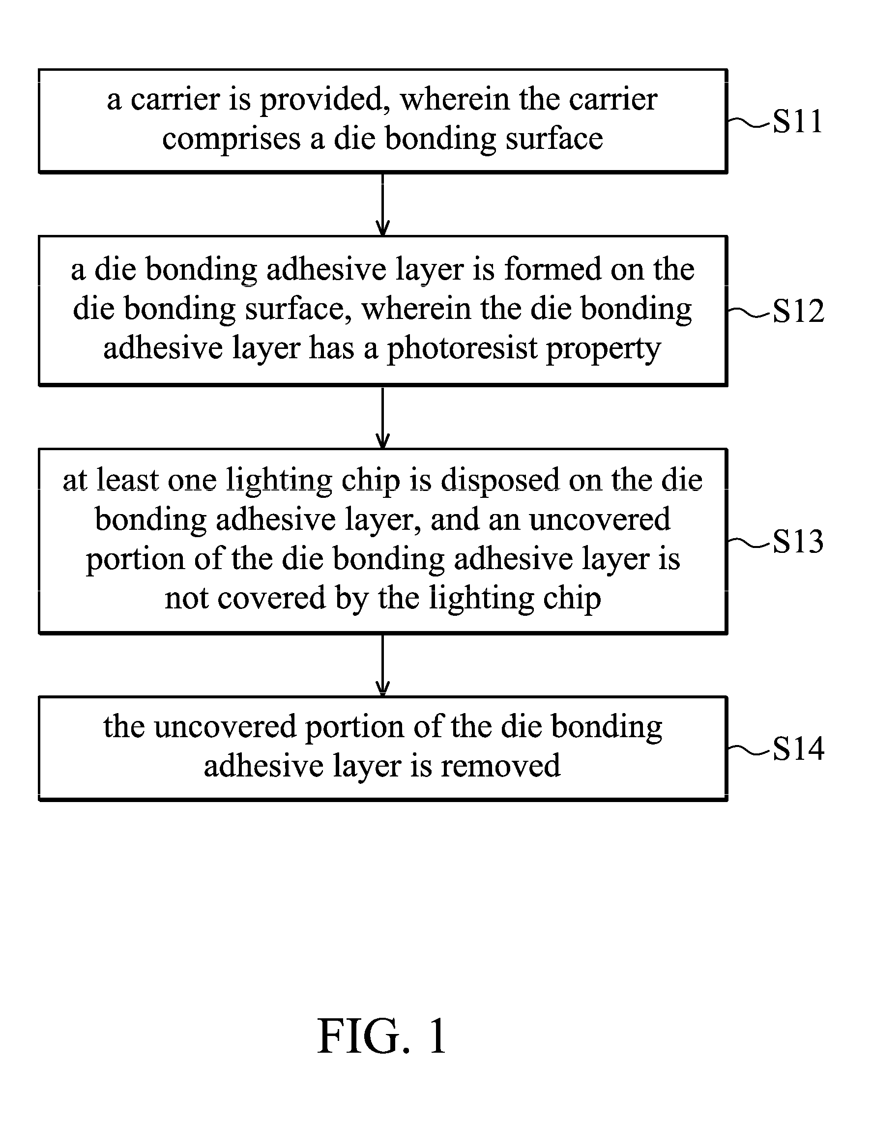
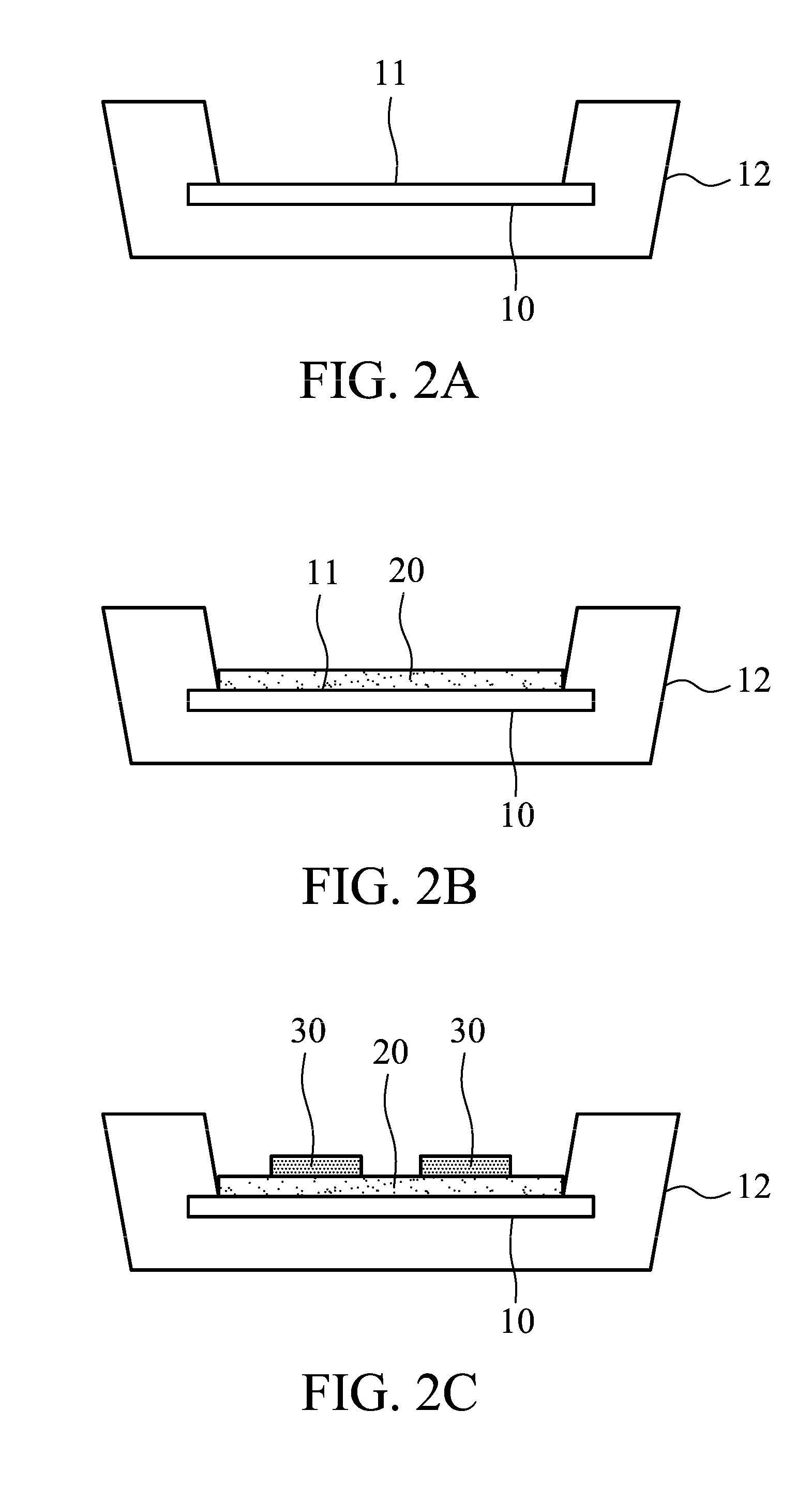
[0016]FIG. 1 shows a method for producing a light-emitting diode of the invention, comprising the following steps. First, a carrier is provided, wherein the carrier comprises a die bonding surface (S11). Then, a die bonding adhesive layer is formed on the die bonding surface, wherein the die bonding adhesive layer has a photoresist property (S12). Next, at least one lighting chip is disposed on the die bonding adhesive layer, and an uncovered portion of the die bonding adhesive layer is not covered by the lighting chip (S13). Finally, the uncovered portion of the die bonding adhesive layer is removed (S14).
[0017]FIG. 2A shows step S11 of the first embodiment of the invention, wherein the carrier 10 comprises the die bonding surface 11. In this embodiment, a plastic cup 12 is provided. The carrier 10 is embedded in the plastic cup 12, and the die bonding surface 11 is uncovered. The carrier 10 comprises metal or metallic oxide to increase heat conductivity.
[0018]FIG. 2B shows step S1...
second embodiment
[0023]FIG. 3 shows a method for producing a light-emitting diode of the invention, comprising the following steps. First, a carrier is provided, wherein the carrier comprises a die bonding surface (S21). Then, a patterned photoresist layer is formed on the die bonding surface, wherein the patterned photoresist layer comprises an opening, and the die bonding surface is uncovered in the opening (S22). Next, a die bonding adhesive layer is formed in the opening (S23). Then, a lighting chip is disposed on the die bonding adhesive layer (S24). Finally, the patterned photoresist layer is removed (S25).
[0024]FIG. 4A shows step S21 of the second embodiment of the invention, wherein the carrier 10 comprises the die bonding surface 11. In this embodiment, a plastic cup 12 is provided. The carrier 10 is embedded in the plastic cup 12, and the die bonding surface 11 is uncovered. The carrier 10 comprises metal or metallic oxide to increase heat conductivity.
[0025]FIGS. 4B˜4D show step S22 of th...
PUM
 Abstract
Description
Claims
Application Information