Compensation circuit for common voltage according to gate voltage

a compensation circuit and gate voltage technology, applied in the direction of differential amplifiers, instruments, amplifiers with semiconductor devices/discharge tubes, etc., can solve the problems of high gate voltage variation, achieve the effect of preventing noise generation, minimizing variation of common voltage, and preventing degradation of picture quality

Active Publication Date: 2015-07-02
LG DISPLAY CO LTD
View PDF5 Cites 11 Cited by
  • Summary
  • Abstract
  • Description
  • Claims
  • Application Information

AI Technical Summary

Benefits of technology

[0033]An advantage of the present invention is to provide a compensation circuit for a common voltage according to a gate voltage, which is capable of minimizing variation in common voltage caused by compensation of a gate high voltage according to variation in temperature, thereby preventing degradation of picture quality caused by variation in common voltage.
[0034]Additional advantages and features of the invention will be set forth in part in the description which follows and in part will become apparent to those having ordinary skill in the art upon examination of the following or may be learned from practice of the invention. The objectives and other advantages of the invention may be realized and attained by the structure particularly pointed out in the written description and claims hereof as well as the appended drawings.
[0035]To achieve these other advantages and in accordance with the purpose of the invention, as embodied and broadly described herein, a compensation circuit for a common voltage according to a gate voltage includes a divider to divide a gate high voltage, an adder to add a fed-back common voltage to a voltage output from the divider, and a differential amplifier to differentially amplify a voltage output from the adder, and to output the amplified voltage as a compensated common voltage.
[0036]The voltage output from the adder may be input to an inverting terminal (−) of the differential amplifier, and a voltage from a variable resistor may be applied to a non-inverting terminal (+) of the differential amplifier.
[0037]The common voltage compensation circuit according to the present invention having the above-described features has the following effects.
[0038]That is, when the gate high voltage is varied in accordance with a variation in ambient temperature, an optimal common voltage is varied in accordance with the gate high voltage variation. Accordingly, it may be possible not only to prevent generation of noise caused by a difference between an optimal common voltage at low temperature and a common voltage set at normal temperature, but also to avoid ripple in the gate high voltage, differently than the conventional case. Thus, an improvement in picture quality may be achieved.

Problems solved by technology

However, variation of gate high voltage in the related art case encounters the following problems.

Method used


Image

  • Compensation circuit for common voltage according to gate voltage
  • Compensation circuit for common voltage according to gate voltage
  • Compensation circuit for common voltage according to gate voltage

Examples


Embodiment Construction

[0046]Reference will now be made in detail to the embodiments of the present invention, examples of which are illustrated in the accompanying drawings.

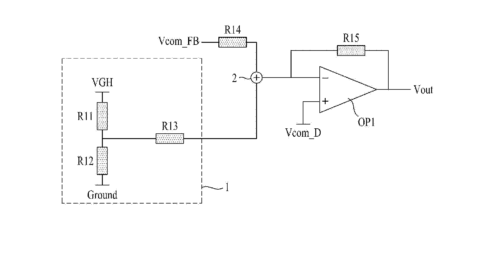
[0047]FIG. 5 is a diagram illustrating a circuit for compensating a common voltage depending on a gate voltage in accordance with the present invention.

[0048]As illustrated in FIG. 5, the compensation circuit includes a divider 1 including a plurality of resistors, for example, resistors R11 and R12, to divide a gate high voltage VGH, an adder 2 to feed back a common voltage output from a common voltage circuit (not shown) (cf. FIG. 2), and to add the fed-back common voltage, namely, a voltage Vcom_FB, to a voltage output from the divider 1, and a differential amplifier OP1 to amplify a difference between a voltage output from the adder 2 and a voltage Vcom_D output from a variable resistor, thereby outputting a compensated common voltage.

[0049]In this case, the voltage output from the adder 2 is input to an inverting terminal (−) of ...


PUM


Abstract

Disclosed is a compensation circuit for a common voltage according to a gate voltage, which compensates the common voltage in accordance with variation in gate high voltage, to obtain an optimal common voltage. The compensation circuit includes a divider to divide a gate high voltage, an adder to add a fed-back common voltage to a voltage output from the divider, and a differential amplifier to differentially amplify a voltage output from the adder, and to output the amplified voltage as a compensated common voltage.

Description

[0001]This application claims the benefit of the Korean Patent Application No. 10-2013-0167586, filed on Dec. 30, 2013, which is hereby incorporated by reference for all purposes as if fully set forth herein.BACKGROUND OF THE INVENTION[0002]1. Field of the Invention[0003]The present invention relates to a liquid crystal display device. More particularly, the present invention relates to a compensation circuit for a common voltage according to a gate voltage, which compensates the common voltage in accordance with variation in a gate high voltage, to obtain an optimal common voltage.[0004]2. Discussion of the Related Art[0005]With the recent progress of an information-dependent society, the field of displays to visually express electric information signals has rapidly developed. As a result, various flat display devices having superior characteristics such as lightness, thinness, and low power consumption have been developed to rapidly replace for cathode ray tubes (CRTs).[0006]Examp...

Claims


Application Information

Patent Timeline
Patent Type & Authority Applications(United States)
IPC IPC(8): G05F1/46H03F3/45
CPCG05F1/461H03F2203/45116H03F2200/129H03F3/45076G09G3/3655G09G2320/0247G09G2320/0276G09G2320/041G09G2330/12G09G3/36
Inventor LEE, KYUNG-WOOSONG, JAE-HUN
Owner LG DISPLAY CO LTD
Why Eureka
Try Eureka