Display Device, and Driving Method and Electronic Device Thereof

a technology of electronic devices and display devices, applied in static indicating devices, electroluminescent light sources, instruments, etc., can solve the problems of inability to perform sharp display with high contrast, and achieve the effects of high contrast, increased peak luminance in the portion, and sharp image display

Inactive Publication Date: 2015-07-02
SEMICON ENERGY LAB CO LTD
View PDF8 Cites 6 Cited by
  • Summary
  • Abstract
  • Description
  • Claims
  • Application Information

AI Technical Summary

Benefits of technology

[0021]One feature of the structure of the display device of the present invention is that the number of sub-frames is decreased when the average gray scale level becomes lower than a predetermined value.
[0052]When an average luminance of an entire screen is low and a high gray scale is displayed in a portion, a peak luminance in the portion can be increased, and a display device capable of performing sharp image display with high contrast can be provided.

Problems solved by technology

Therefore, sharp display with high contrast cannot be performed.

Method used


Image

  • Display Device, and Driving Method and Electronic Device Thereof
  • Display Device, and Driving Method and Electronic Device Thereof
  • Display Device, and Driving Method and Electronic Device Thereof

Examples


embodiment mode 1

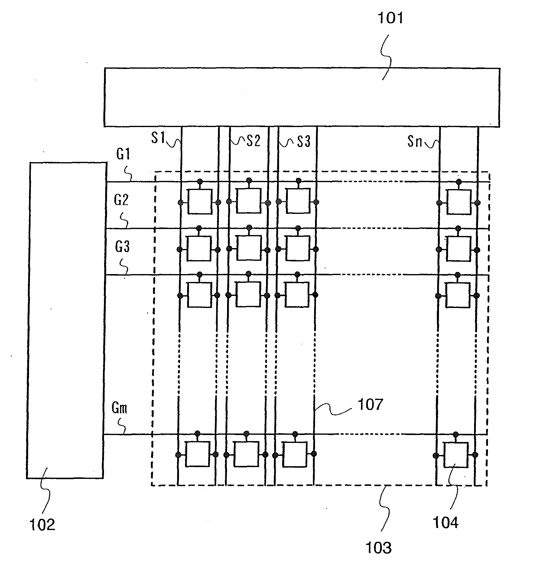
[0094]FIG. 1 shows a basic pixel matrix circuit of a display device of the present invention. This pixel matrix circuit includes a signal line driver circuit 101, a scanning line driver circuit 102, and a pixel portion 103 which is provided with a plurality of pixels 104. In addition, corresponding to scanning lines (G1 to Gm) disposed in rows, signal lines (S1 to Sn) disposed in columns, and power supply lines 107, pixels 104 are disposed in matrix.

[0095]The signal line driver circuit 101 outputs a video signal to the signal lines S1 to Sn. The scanning line driver circuit 102 outputs a signal for selecting the pixels 104 disposed in rows, to the scanning lines G1 to Gm. Then, the video signal from the signal line driver circuit 101 is written in each pixel 104 of a pixel row selected by the signal that is output from the scanning line driver circuit 102. Note that the signal input to the signal lines S1 to Sn from the signal line driver circuit 101 is not limited to a video signal...

embodiment mode 2

[0144]An operation method of Embodiment Mode 2 will be described with reference to a timing chart of FIG. 8 where a 4-bit gray scale is expressed. The signal writing operation is performed from a first row to an m-th row. Then, a sustain period starts in the row in which the writing operation has been terminated. The next sub-frame starts sequentially in the row in which the sustain period has been terminated, and the signal writing operation is carried out again from the first row. Here, a signal erasing operation is carried out between one signal writing operation and the next signal writing operation, so as to provide a non-lighting period. By providing the signal erasing operation as described above, a sustain period is controlled.

[0145]A circuit configuration of a pixel which is operated in the above-described manner is shown in FIG. 9. A driving TFT 901, a switching TFT 902, a capacitor 903, a light emitting element 904, a first scanning line 905, a signal line 906, a power su...

embodiment mode 3

[0158]In Embodiment Mode 3, the case where a signal erasing operation of a pixel is performed with a pixel configuration different from that in Embodiment Mode 2 will be described.

[0159]FIG. 10 shows one example of a pixel configuration in the case the driving TFI is forcibly turned off. A switching TFI 1002, a driving TFT 1001, an erasing diode 1009, and a light emitting element 1004 are provided. One of a source region and a drain region of the switching TFT 1002 is connected to a signal line 1006, and the other is connected to a gate electrode of the driving TFT 1001, the capacitor 1003, and the erasing diode 1009. A gate electrode of the switching TFT 1002 is connected to a first scanning line 1005. One of a source region and a drain region of the driving TFT 1001 is connected to a power supply line 1007, and the other is connected to the light emitting element 1004. An input terminal of the erasing diode 1009 is connected to a second scanning line 1010, and an output terminal o...


PUM


Abstract

By controlling gray scale of a display device in accordance with an average luminance of a display screen, sharp display is performed. In addition, it is an object to provide a display device with reduced deterioration of a light emitting element, by the control in accordance with the average luminance of a display screen so as to perform display appropriately. A display which includes a plurality of pixels each including a light emitting element, a switching TFT and a driving TFT, an average gray scale calculation circuit which calculates an average luminance of all pixels in a frame period, a sub-frame-number control circuit which controls the number of sub-frames in accordance with the calculated average luminance level, and a potential control circuit which controls a potential applied to both ends of a light emitting element in accordance with the calculated average luminance level are included.

Description

BACKGROUND OF THE INVENTION[0001]1. Field of the Invention[0002]The present invention relates to a display device on which an EL (electroluminescent) element, an organic EL element, or another self-emission type display element is mounted. In addition, the present invention relates to a driving method of the display device. Further, the present invention relates to an electronic device provided with the display device in a display portion.[0003]2. Description of the Related Art[0004]In recent years, a so-called self-emission type display device in which a pixel is formed by using a light emitting element such as a light emitting diode (LED), has been the focus of recent interest. As a light emitting element used in such a self-emission type display device, an organic light emitting diode (also referred to as an OLED (Organic Light Emitting Diode), an organic EL element, an electroluminescence (EL) element, or the like) attracts attention and is increasingly used in an EL display or ...

Claims


Application Information

Patent Timeline
Patent Type & Authority Applications(United States)
IPC IPC(8): G09G3/20G09G3/32H05B44/00
CPCG09G3/2014G09G3/3258G09G3/2022G09G2300/0842G09G2360/16G09G2310/06G09G2320/043G09G2320/0626G09G2300/0866G09G3/30G09G3/20G09G3/32
Inventor KIMURA, HAJIME
Owner SEMICON ENERGY LAB CO LTD
Why Eureka
Try Eureka