Printed circuit board device

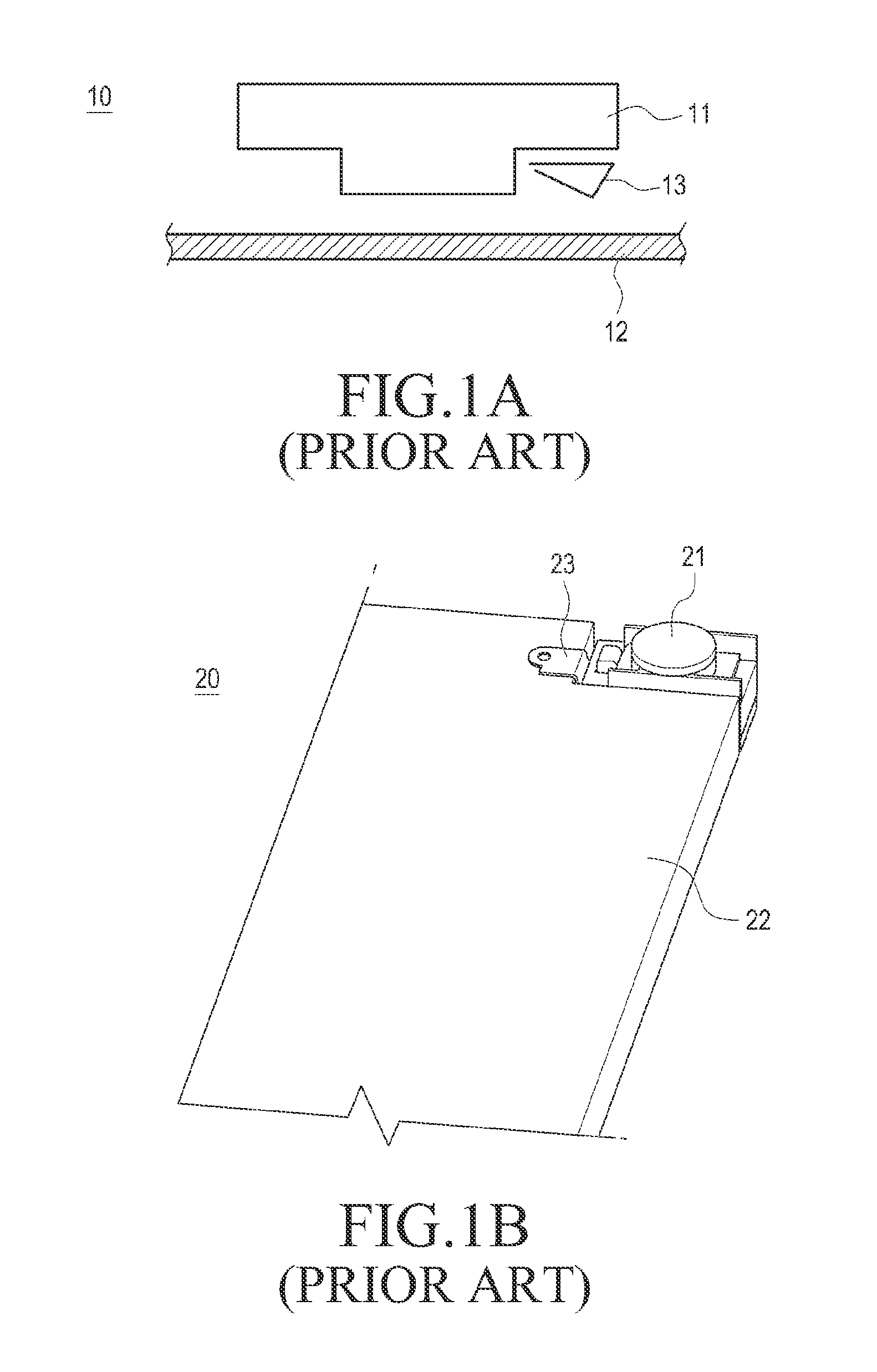
a printed circuit board and elastic member technology, applied in the direction of coupling contact members, coupling device connections, printed circuits, etc., can solve the problems of difficult work of wire-type connectors, low contact stability of connector types, and bulky circuit board devices, so as to reduce the thickness of parts and the circuit board, the manufacturing process is simplified, and the assembly or disassembly process is easy.

Active Publication Date: 2015-07-23
SAMSUNG ELECTRONICS CO LTD
View PDF12 Cites 0 Cited by
  • Summary
  • Abstract
  • Description
  • Claims
  • Application Information

AI Technical Summary

Benefits of technology

[0012]Accordingly, an aspect of the present invention is to provide a circuit board device that enables electronic components and circuit boards to be installed at various positions.
[0013]Another aspect of the present invention is to provide a circuit board device that may provide easy assembly or disassembly together with a simplified manufacturing process.
[0014]Another aspect of the present invention is to provide a circuit board device that may diversify the position of the interconnect terminal of the part and the installed direction of the interconnect terminal of the circuit board.
[0015]Another aspect of the present invention is to provide a circuit board device that may reduce the installed thickness of the part and the circuit board.

Problems solved by technology

Such stacking may leave the circuit board device bulky.
However, this connector type has a lower contact stability compared with the contact-type connector, and it requires a separate member (e.g., soldering) for secure mating between the electronic component and the circuit board.
Accordingly, the wire-type connector is difficult to work with because of, for example, difficult assembling or disassembling the connector, the electronic component, and the circuit board.
However, the use of the flexible circuit board may result in increased costs.

Method used


Image

  • Printed circuit board device
  • Printed circuit board device
  • Printed circuit board device

Examples


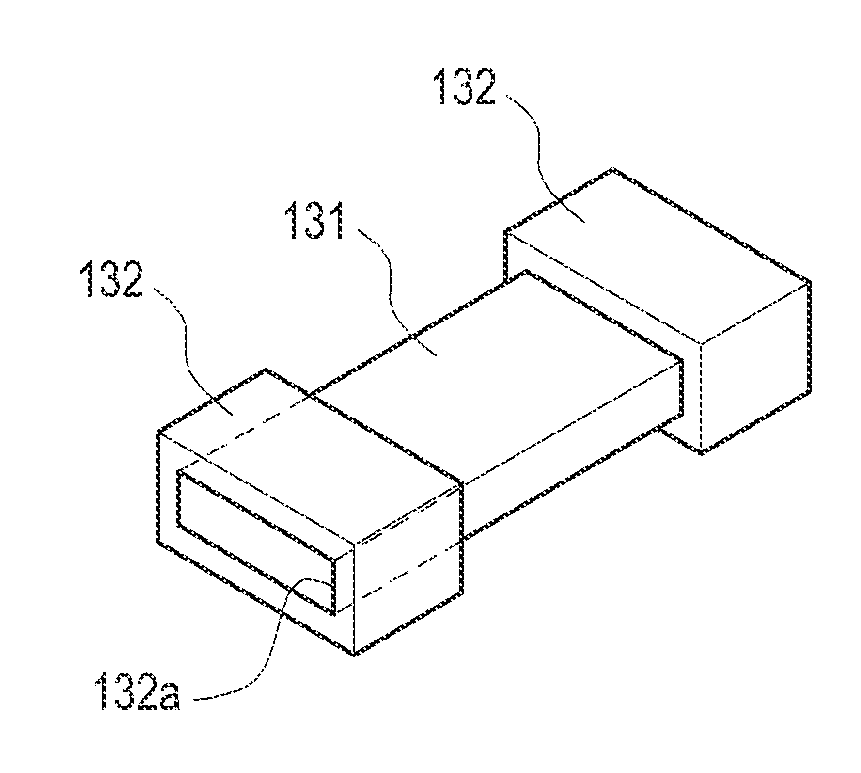
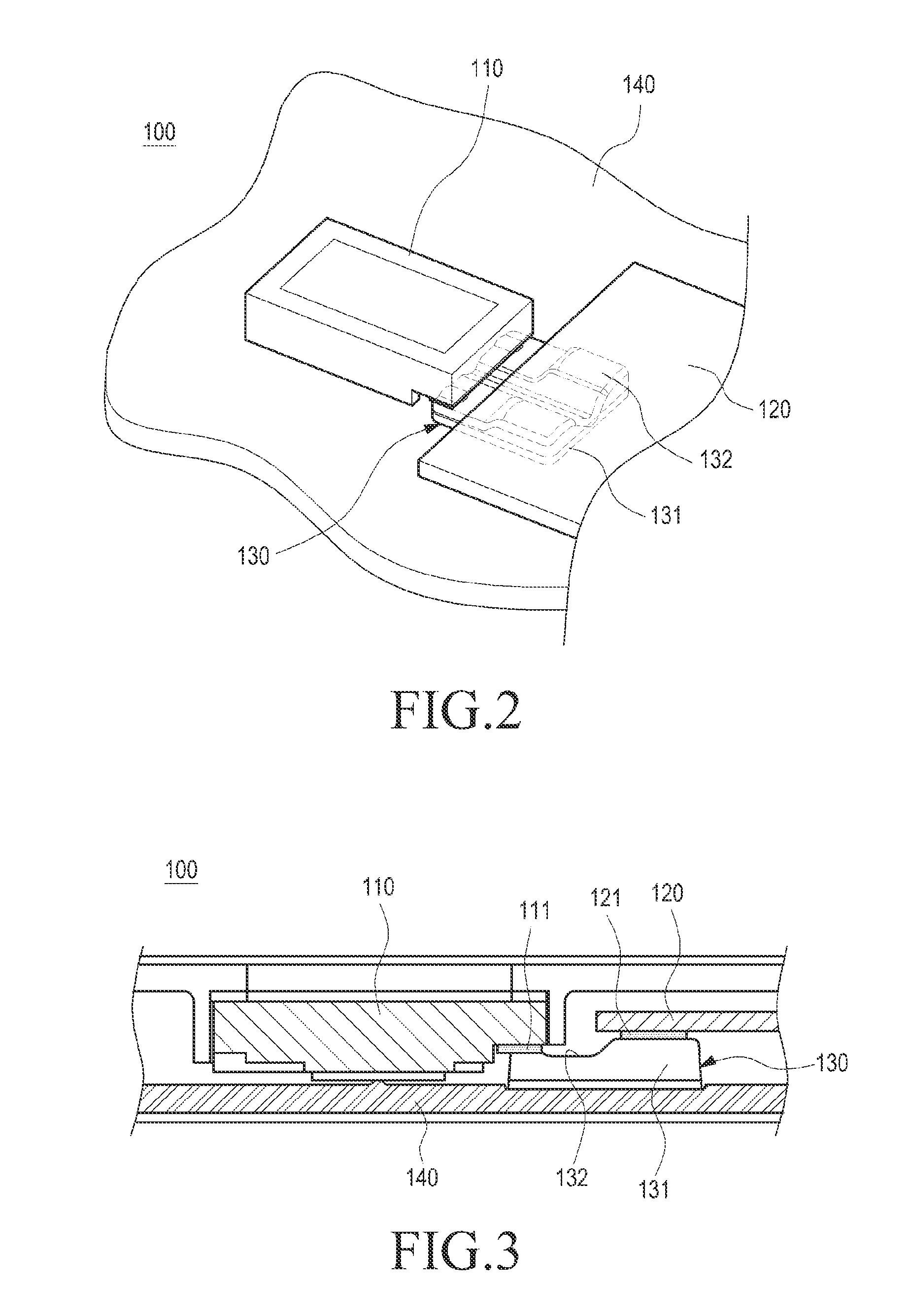
Embodiment Construction

[0038]Hereinafter, various embodiments of the present invention are described in detail with reference to the accompanying drawings. When determined to make the subject matter of the present invention unclear, the detailed description of the known art or functions may be omitted. The terms as used herein are defined considering the functions in specific embodiments of the present invention and may be replaced with other terms according to the user's intention or custom. The terms may be more clearly defined by the description of various embodiments of the present invention. As used herein, the terms “first” and “second” are provided merely to distinguish components of the same name from each other, and the components may be referenced to have other various orders.

[0039]As used hereinafter, the term “electronic device” may be referred to as a terminal, a portable terminal, a mobile terminal, a communication terminal, a portable communication terminal, a portable mobile terminal, or a...


PUM


Abstract

A printed circuit board (PCB) device is provided, which includes a base board, a part, and a conductive elastic member configured to electrically connect the base board with the part. The conductive elastic member comprises a non-conductive body and at least one conductive interconnect port provided on the non-conductive body and configured to electrically connect an interconnect terminal of the base board with an interconnect terminal of the part.

Description

PRIORITY[0001]This application claims priority under 35 U.S.C. §119(a) to a Korean Patent Application filed in the Korean Intellectual Property Office on Jan. 20, 2014 and assigned Serial No. 10-2014-0006718, the entire content of which is incorporated herein by reference.BACKGROUND[0002]1. Field of the Invention[0003]The present invention generally relates to printed circuit boards (PCBs), and more specifically, to circuit board devices having conductive elastic members with various shapes and structures.[0004]2. Description of the Related Art[0005]A printed circuit board (PCB) is used in electronics to electrically connect various electronic components or parts, such as integrated circuits (ICs), resistors, switches, or other modularized electronic parts. Connectors for connecting electronic parts to PCBs may be classified into contact types and wire types.[0006]FIG. 1 A schematically illustrates a conventional contact-type connector. FIG. 1B schematically illustrates a convention...

Claims


Application Information

Patent Timeline
Patent Type & Authority Applications(United States)
IPC IPC(8): H01R12/71
CPCH01R12/716H01R12/718H01R13/24
Inventor HAN, JUNG-EUNSHIN, YUN-SUNGHWANG, HO-CHUL
Owner SAMSUNG ELECTRONICS CO LTD
Why Eureka
Try Eureka