Bonding pad structure and touch panel

a technology of bonding pad and touch panel, which is applied in the direction of instruments, conductors, computing, etc., can solve the problem of difficulty in reducing the cost of capacitance touch panel

Inactive Publication Date: 2015-09-10
WISTRON CORP
View PDF2 Cites 18 Cited by
  • Summary
  • Abstract
  • Description
  • Claims
  • Application Information

AI Technical Summary

Benefits of technology

[0007]The invention provides a touch panel, and the config

Problems solved by technology

Consequently, the number of disposed bonding pads increases, causing it difficult to reduce the area required for the circuit board to be bonded to the

Method used


Image

  • Bonding pad structure and touch panel
  • Bonding pad structure and touch panel
  • Bonding pad structure and touch panel

Examples


first embodiment

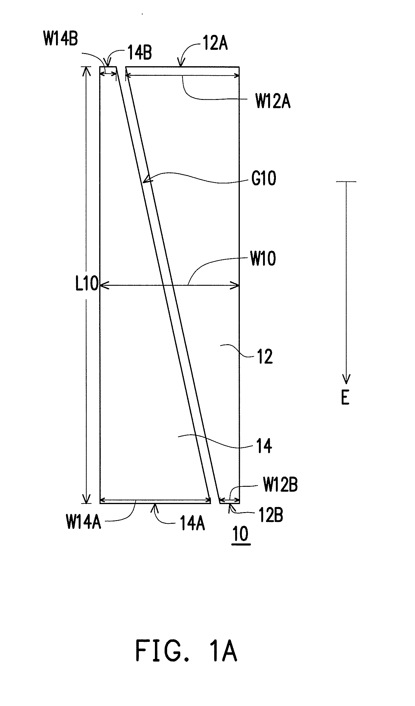
[0044]FIG. 1A is a schematic view illustrating a first embodiment for a bonding pad structure of the invention. Please refer to FIG. 1A. A bonding pad structure 10 includes a first sub-bonding pad 12 independent from a second sub-bonding pad 14, and they are spaced from each other by a gap G10. The first sub-bonding pad 12 has a first connection terminal 12A opposite to a first end terminal 12B. A width W12A of the first connection terminal 12A is greater than a width W12B of the first end terminal 12B. The second sub-bonding pad 14 has a second connection terminal 14A opposite to a second end terminal 14B, and a width 14A of the second connection terminal 14A is greater than a width W14B of the second end terminal 14B. In the meantime, the wider first connection terminal 12A is closer to the narrower second end terminal 14B and farther from the wider second connection terminal 14A. When the bonding pad structure 10 is applied in an electronic device as a bonding pad for bonding, th...

second embodiment

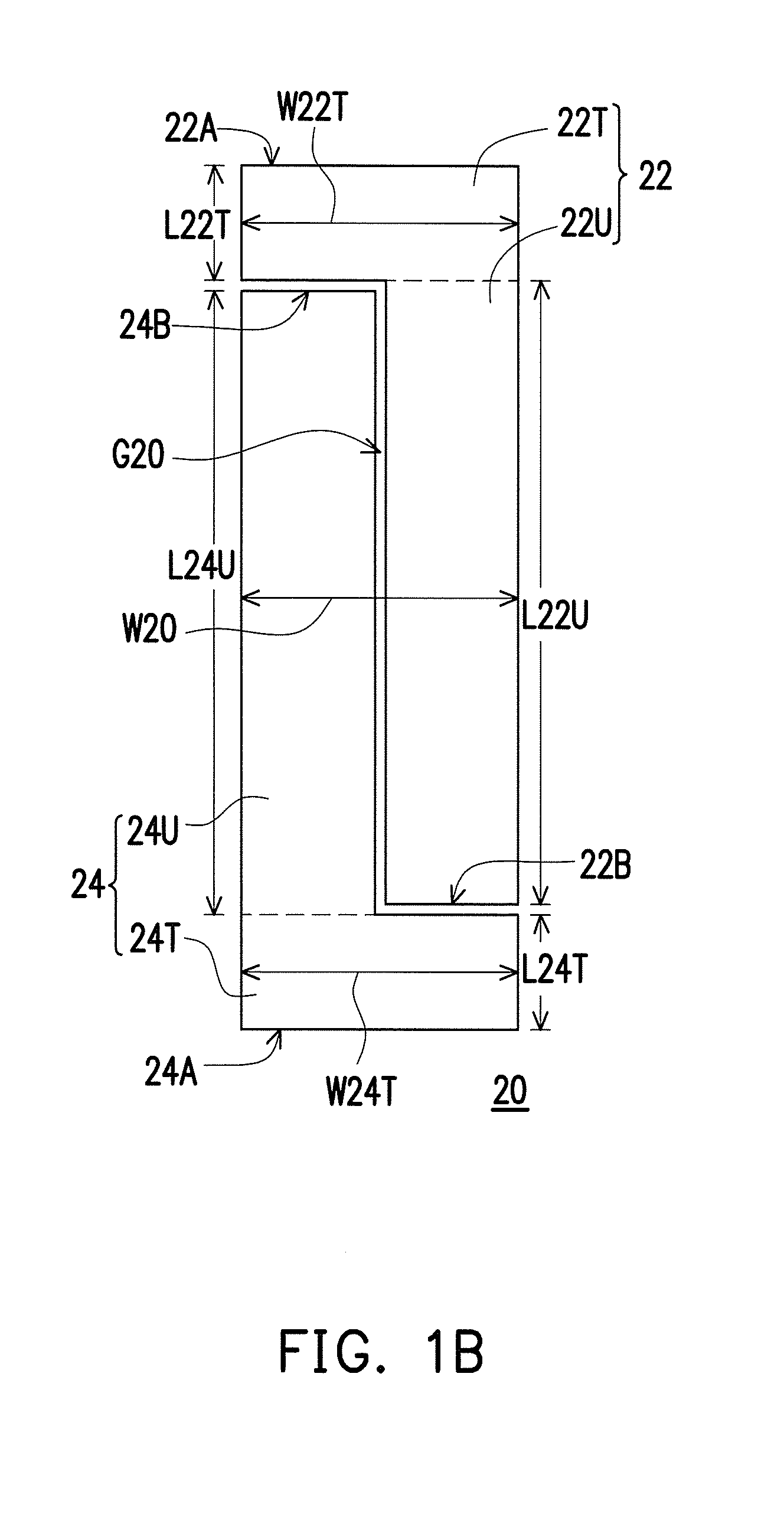
[0048]FIG. 1B is a schematic view illustrating a second embodiment for the bonding pad structure of the invention. Please refer to FIG. 1B. A bonding pad structure 20 includes a first sub-bonding pad 22 independent from a second sub-bonding pad 24, and they are spaced from each other by a gap G20. The first sub-bonding pad 22 of the bonding pad structure 20 includes a first testing portion 22T adjacent to a first bonding portion 22U. A first connection terminal 22A is an end of the first testing portion 22T away from the first bonding portion 22U; a first end terminal 22B is an end of the first bonding portion 22U away from the first testing portion 22T. The second sub-bonding pad 24 includes a second testing portion 22T adjacent to a second bonding portion 24U.

[0049]The second connection terminal 22A is an end of the second testing portion 22T away from the second bonding portion 22U; the second end terminal 24B is an end of the second bonding portion 22U away from the second testi...

third embodiment

[0052]FIG. 1C is a schematic view illustrating a third embodiment for the bonding pad structure of the invention. Please refer to FIG. 1C. A bonding pad structure 30 includes a first sub-bonding pad 32 independent from a second sub-bonding pad 34. The first sub-bonding pad 32 includes a first testing portion 32T and a first bonding portion 32U, and the second sub-bonding pad 34 includes a second testing portion 34T and a second bonding portion 34U. Here, the first testing portion 32T and the first bonding portion 32U are similar to the first testing portion 22T and the first bonding portion 22U of FIG. 1B. The second testing portion 34T and the second bonding portion 34U are similar to the second testing portion 24T and the second bonding portion 24U of FIG. 1B. The two embodiments are different in that a gap G30 between the first bonding portion 32U and the second bonding portion 34U of the embodiment is in a bended shape, whereas the gap G20 between the first bonding portion 22U a...


PUM


Abstract

A bonding pad structure including a first sub-bonding pad and a second sub-bonding pad and a touch panel are provided. The first sub-bonding pad has a first connection terminal at an opposite side of a first end terminal. A width of the first connection terminal is greater than a width of the first end terminal. The first sub-bonding pad has a second connection terminal at an opposite side of a second end terminal. A width of the second connection terminal is greater than a width of the second end terminal. The first connection terminal is close to the second end terminal and the second connection terminal is close to the first end terminal. A first outline of the first sub-bonding pad and a second outline of the second sub-bonding pad are formed as a pair in a complementary manner to construct a configuration of the bonding pad structure.

Description

CROSS-REFERENCE TO RELATED APPLICATION[0001]This application claims the priority benefit of China application serial no. 201410079596.9, filed on Mar. 5, 2014. The entirety of the above-mentioned patent application is hereby incorporated by reference herein and made a part of this specification.BACKGROUND OF THE INVENTION[0002]1. Field of the Invention[0003]The invention is related to a touch sensing device and a bonding structure thereof, and more particularly to a touch panel and a bonding pad structure thereof.[0004]2. Description of Related Art[0005]Touch panels are roughly grouped into resistive touch panels, capacitive touch panels, optical touch panels, acoustic wave touch panels and electromagnetic touch panels according to different sensing principles thereof. The capacitive touch panel is characterized by short response speed, favorable reliability, satisfactory durability, and so on. Therefore, the capacitive touch panel is widely used in the electronic products. Moreover...

Claims


Application Information

Patent Timeline
IPC IPC(8): G06F3/044G06F1/16H01B5/00
CPCG06F3/044G06F1/16H01B5/00G06F2203/04111G06F3/0443G06F3/0446
Inventor LIANG, RAYLIU, ZHENG-XIANGTENG, FEI
Owner WISTRON CORP
Why Eureka
Try Eureka