

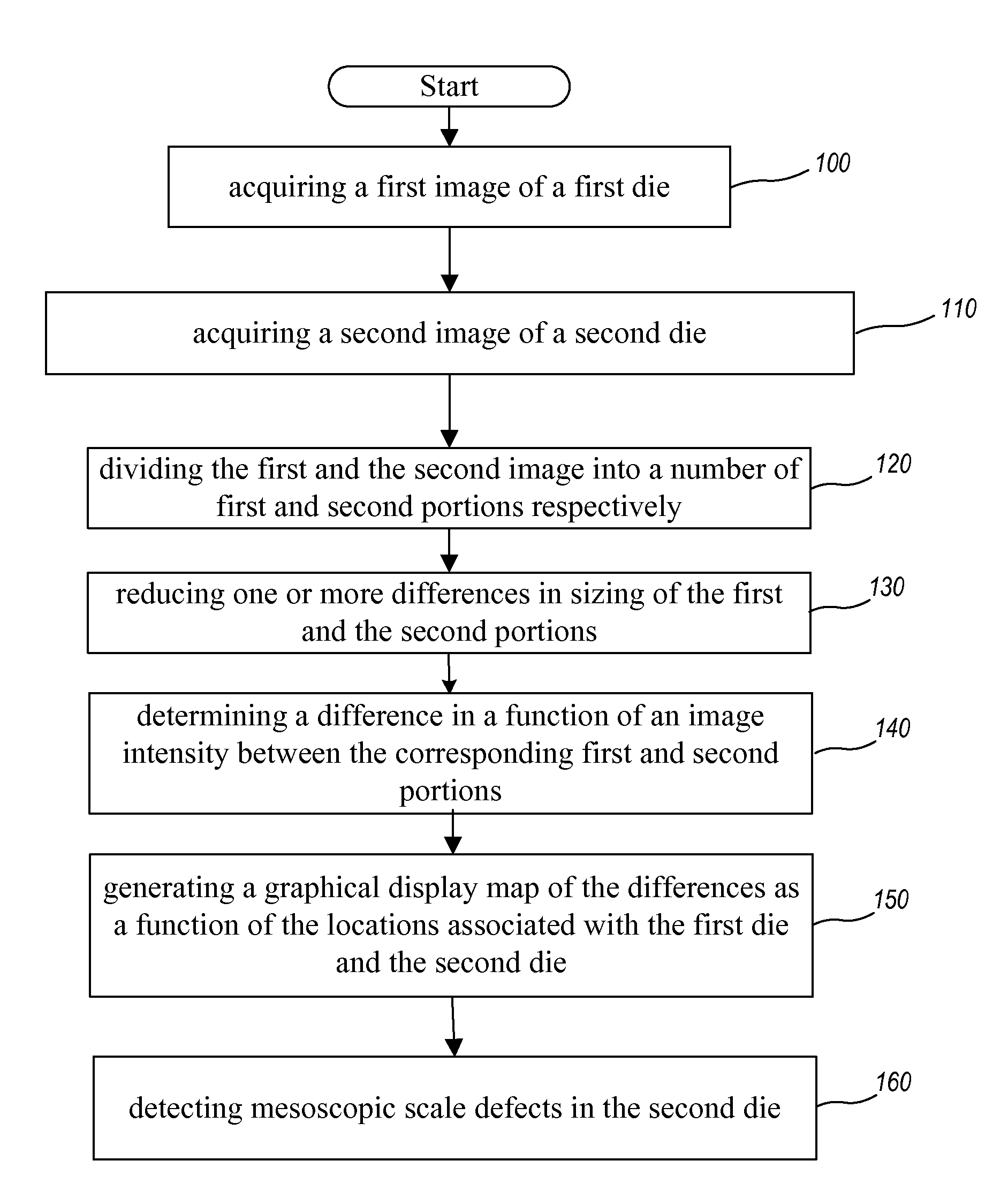
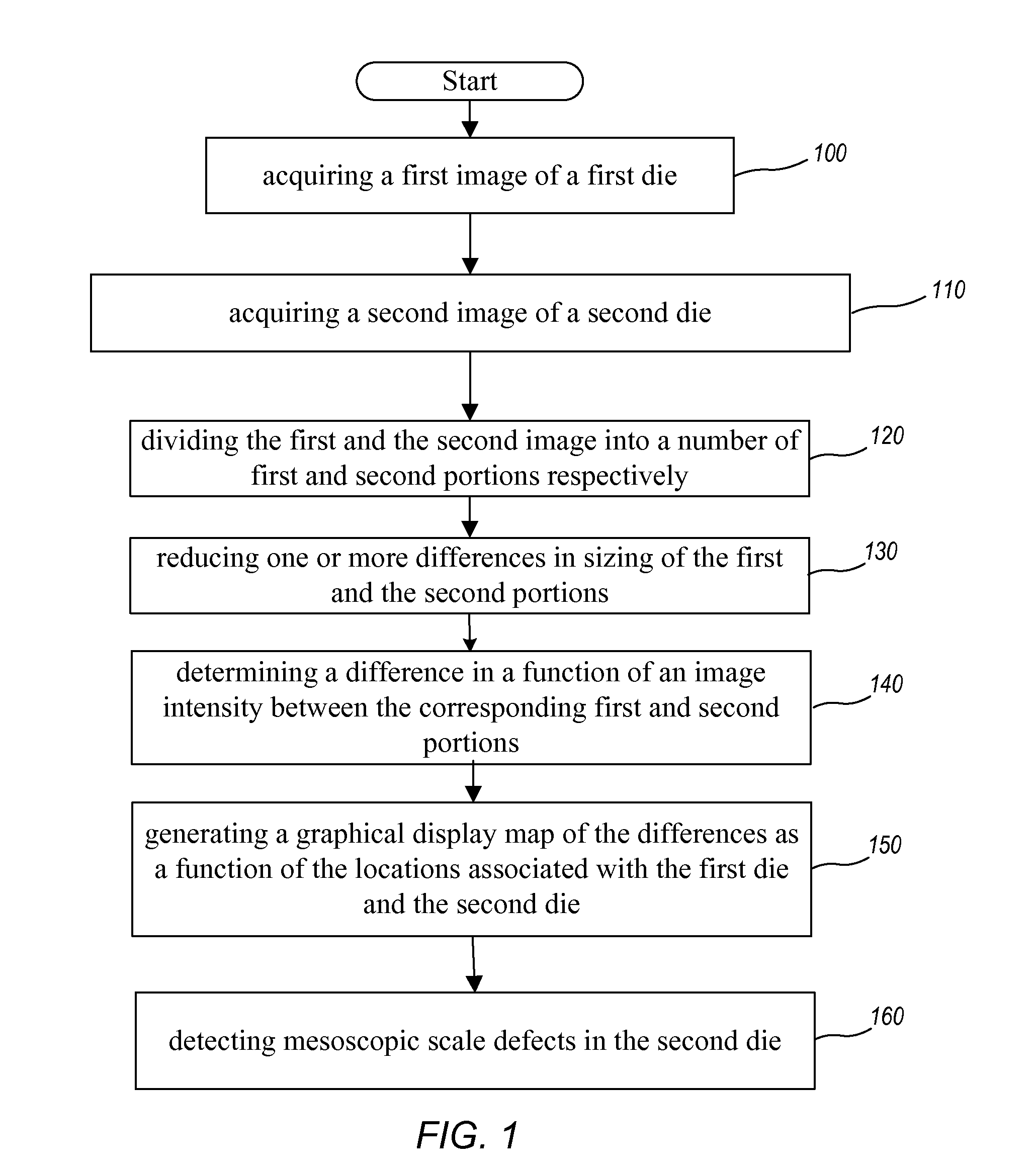
Mesoscopic defect detection for reticle inspection
a technology of reticle and defect detection, applied in the field of detecting defects in reticles or photomasks, can solve the problems of existing methods that do not have the capability or sensitivity to detect defects, defects on reticles or photomasks are detrimental to the yield of semiconductor wafers in the semiconductor manufacturing process, and mesoscopic defects, so as to reduce one or more differences in sizing, reduce any difference in sizing of the first and the second portion, and reduce one or more differences
- Summary
- Abstract
- Description
- Claims
- Application Information
AI Technical Summary
Benefits of technology
Problems solved by technology
Method used
Image


Examples
Embodiment Construction
Definitions
[0023]Unless defined otherwise, all technical and scientific terms used herein have the same meaning as commonly understood by one of ordinary skill in the art.
[0024]The term “connected” as used herein generally refers to pieces which may be joined or linked together.
[0025]The term “coupled” as used herein generally refers to pieces which may be used operatively with each other, or joined or linked together, with or without one or more intervening members.
[0026]The term “directly” as used herein generally refers to one structure in physical contact with another structure, or, when used in reference to a procedure, means that one process affects another process or structure without the involvement of an intermediate step or component.
[0027]The term “mesoscopic” as used herein generally refers to length scales on the order of 103 nm to 102 μm. For example herein there may be made reference to mesoscopic defects meaning defects on the order of 103 nm to 102 μm in the lateral...
PUM
 Abstract
Description
Claims
Application Information