Semiconductor device, semiconductor system and method for operating semiconductor device

a semiconductor and semiconductor technology, applied in the direction of generating/distributing signals, pulse automatic control, instruments, etc., can solve the problems of power consumption, power consumption, and increase in the operation speed of the semiconductor circuit, so as to minimize power consumption and high operation speed

Active Publication Date: 2015-11-19
SK HYNIX INC
View PDF0 Cites 4 Cited by
  • Summary
  • Abstract
  • Description
  • Claims
  • Application Information

AI Technical Summary

Benefits of technology

[0016]Also according to the embodiments, since an operation speed of a semiconductor device is determined based on a work load, the op

Problems solved by technology

In portable devices that use batteries, power consumption is battery leading factor in determining battery life.
As the clock signal frequency in a semiconductor circuit increases in conjunction with a high voltage power supply, the operation speed of the semiconductor c

Method used


Image

  • Semiconductor device, semiconductor system and method for operating semiconductor device
  • Semiconductor device, semiconductor system and method for operating semiconductor device
  • Semiconductor device, semiconductor system and method for operating semiconductor device

Examples


Embodiment Construction

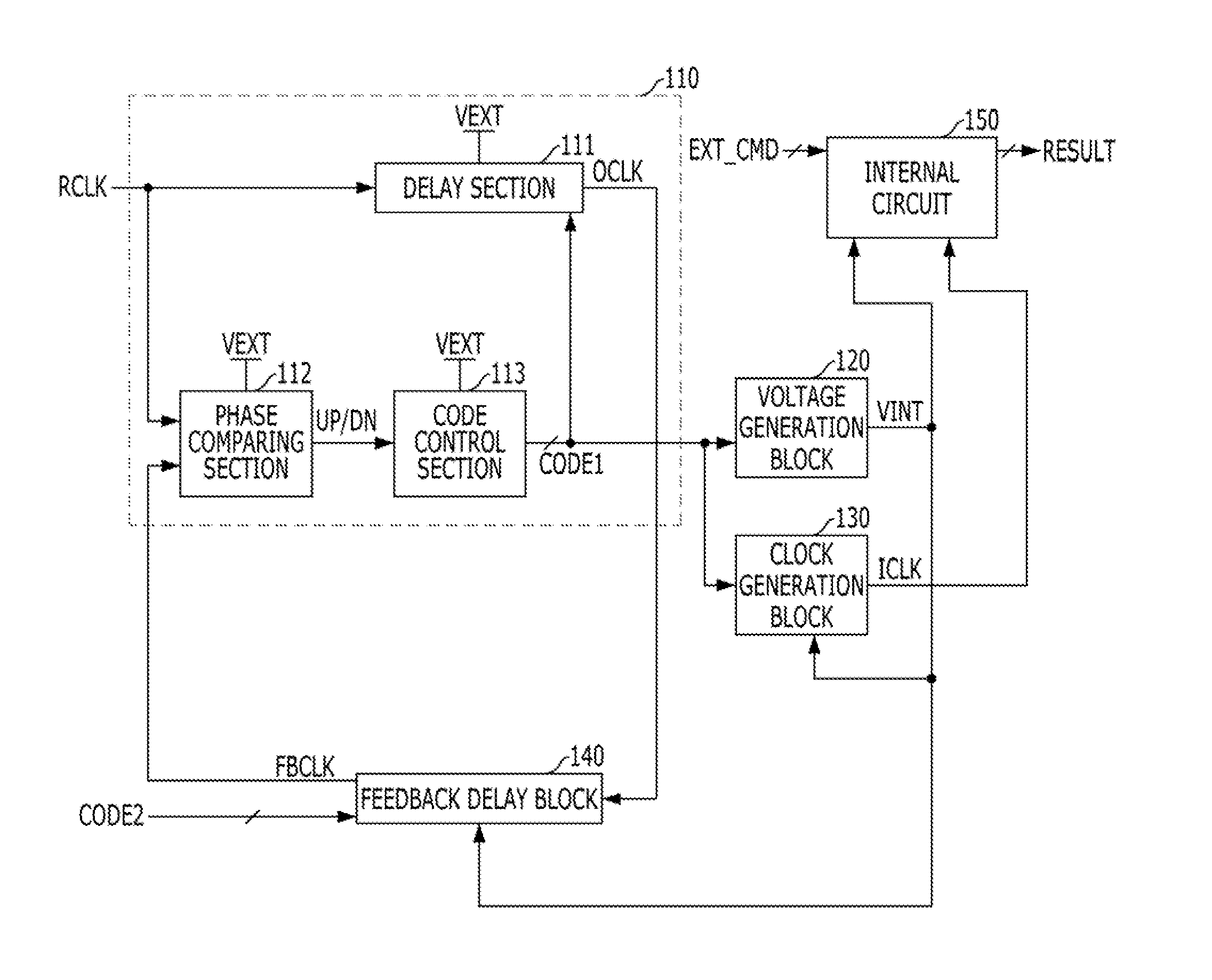
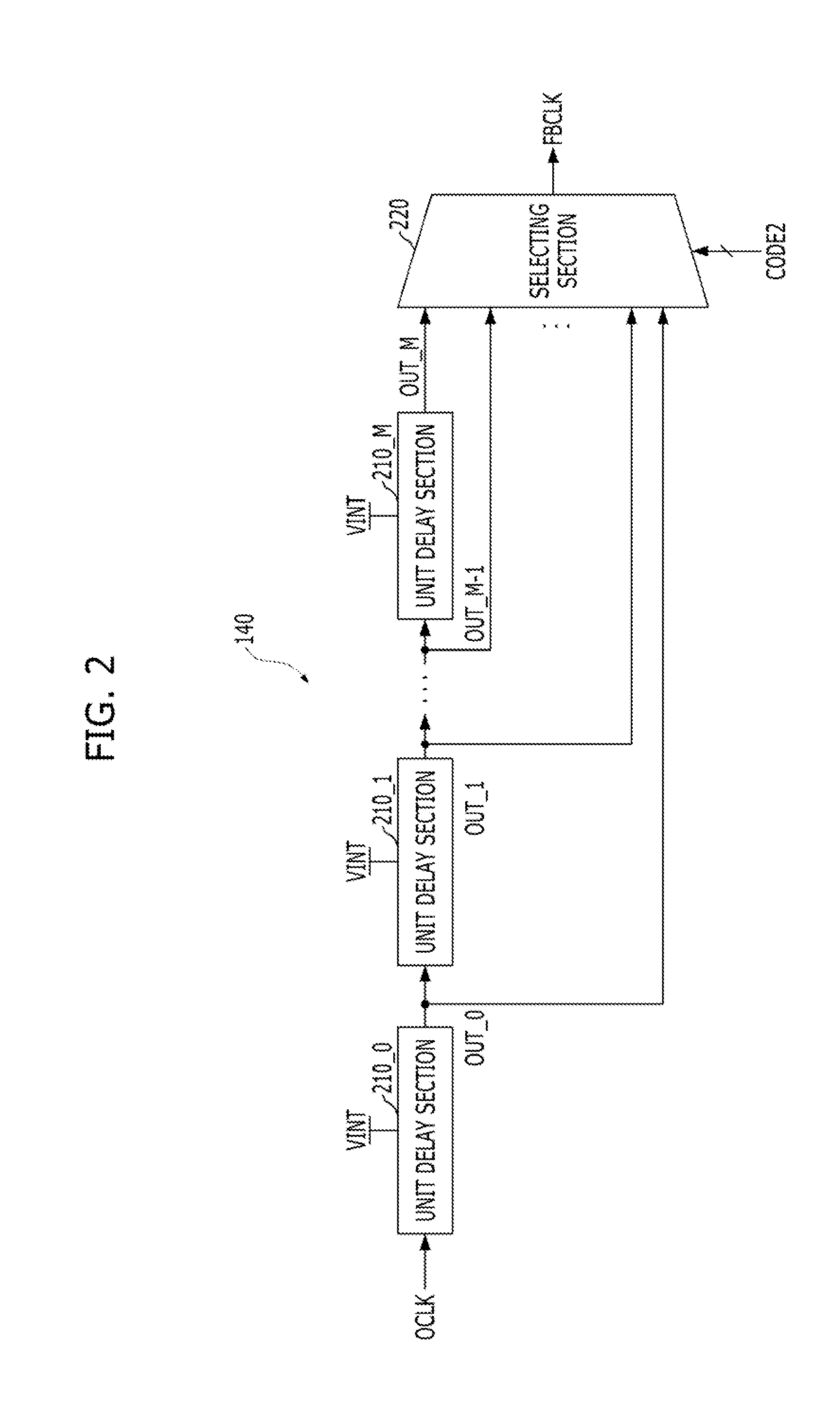
[0022]Various embodiments will be described below in more detail with reference to the accompanying drawings. The present invention may, however, be embodied in different forms and should not be construed as limited to the embodiments set forth herein. Rather, these embodiments are provided so that this disclosure will be thorough and complete, and will fully convey the scope of the present invention to those skilled in the art. Throughout the disclosure, like reference numerals refer to like parts throughout the various figures and embodiments of the present invention.

[0023]In the drawings, a thickness and length of components are exaggerated for convenience of illustration. In the following description, a detailed explanation of known related functions and constitutions may be omitted to avoid unnecessarily obscuring the subject manner of the present invention. Furthermore, ‘connected / coupled’ represents that one component is directly coupled to another component or indirectly cou...


PUM


Abstract

A semiconductor device includes a code generation block configured to generate an output clock by delaying a reference clock which is inputted from an exterior, control a delay value of the output clock based on a result of comparing phases of the reference clock and a feedback clock, and generate a first control code corresponding to the delay value of the output clock, a voltage generation block configured to generate an internal voltage with a voltage level corresponding to the first control code, a clock generation block configured to generate an internal clock with a frequency corresponding to the first control code, and a feedback delay block configured to generate the feedback clock by delaying the output clock by a delay value corresponding to a second control code.

Description

CROSS-REFERENCE TO RELATED APPLICATIONS[0001]The present application claims priority of Korean Patent Application No. 10-2014-0059618, filed on May 19, 2014, which is incorporated herein by reference in its entirety.BACKGROUND[0002]1. Field[0003]This patent document relates to a semiconductor device, a semiconductor system, and a method for operating the semiconductor device.[0004]2. Description of the Related Art[0005]A system-on-chip (SoC) is a technology that incorporates various function blocks such as a CPU (central processing unit), a memory, an interface, a digital signal processing circuit and an analog signal processing circuit in one semiconductor integrated circuit. Application examples of SoCs include computer systems, electronic systems, and integrated circuits (IC) fabricated for various electronic devices.[0006]The SoC is being developed with more complicated systems by absorbing various functions associated with processors, multimedia, graphics, interfaces and securi...

Claims


Application Information

Patent Timeline
IPC IPC(8): H03L7/08H03L7/10H03K3/86H03L7/083
CPCH03L7/0802H03L7/083H03L7/10H03K3/86H03L7/0814G06F1/3296H03L7/0816G06F1/08G06F1/324G11C7/222G11C29/023G11C29/028H03L7/0805
Inventor JUNG, JI-WAN
Owner SK HYNIX INC
Why Eureka
Try Eureka