Termination of high voltage (HV) devices with new configurations and methods

a technology of high voltage and configuration, applied in the direction of semiconductor devices, basic electric elements, electrical apparatus, etc., can solve the problems of limited support voltage, reduce the crowding effect of electrical fields, reduce the resistance of surface charge, and reduce the effect of surface electric field

Inactive Publication Date: 2016-01-14
LEE YEEHENG +4
View PDF15 Cites 10 Cited by
  • Summary
  • Abstract
  • Description
  • Claims
  • Application Information

AI Technical Summary

Benefits of technology

[0007]It is therefore an aspect of the present invention to provide a new and improved edge termination configuration to reduce the electrical field crowding effects near the blocking junction at the device edge and provide a compact termination with lower surface electric field that is less sensitive to surface charge. This is achieved with the formation of a plurality of termination trenches formed in the heavily doped region and forming doped regions at the bottom of the termination trenches in the lightly doped region to function as buried guard rings in the edge termination.

Problems solved by technology

The termination trenches with no guard ring doped region do not have the P-region along the sidewalls and can therefore sustain high breakdown voltage limited by the buried guard ring pinch-off.

Method used


Image

  • Termination of high voltage (HV) devices with new configurations and methods
  • Termination of high voltage (HV) devices with new configurations and methods
  • Termination of high voltage (HV) devices with new configurations and methods

Examples


Embodiment Construction

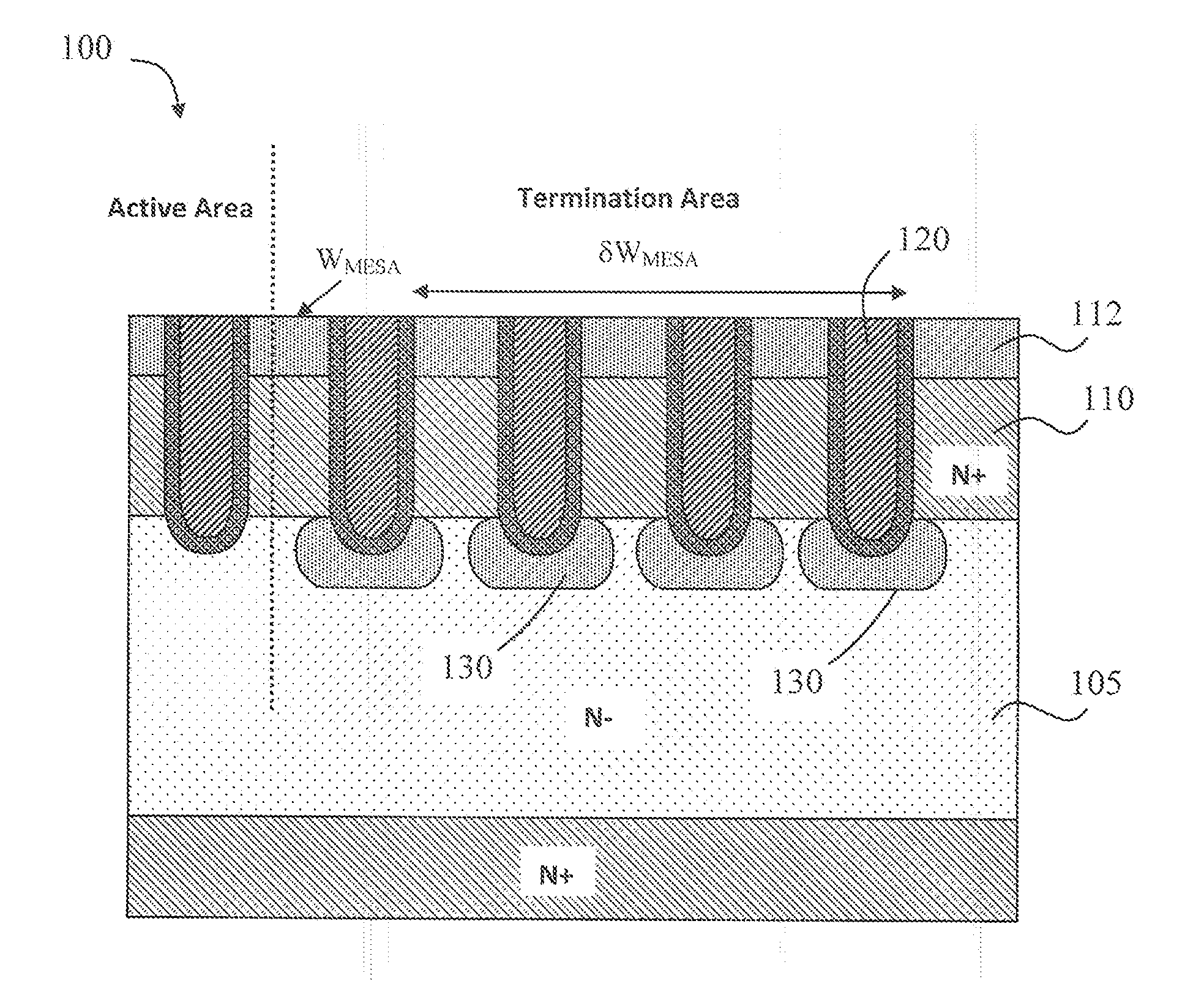
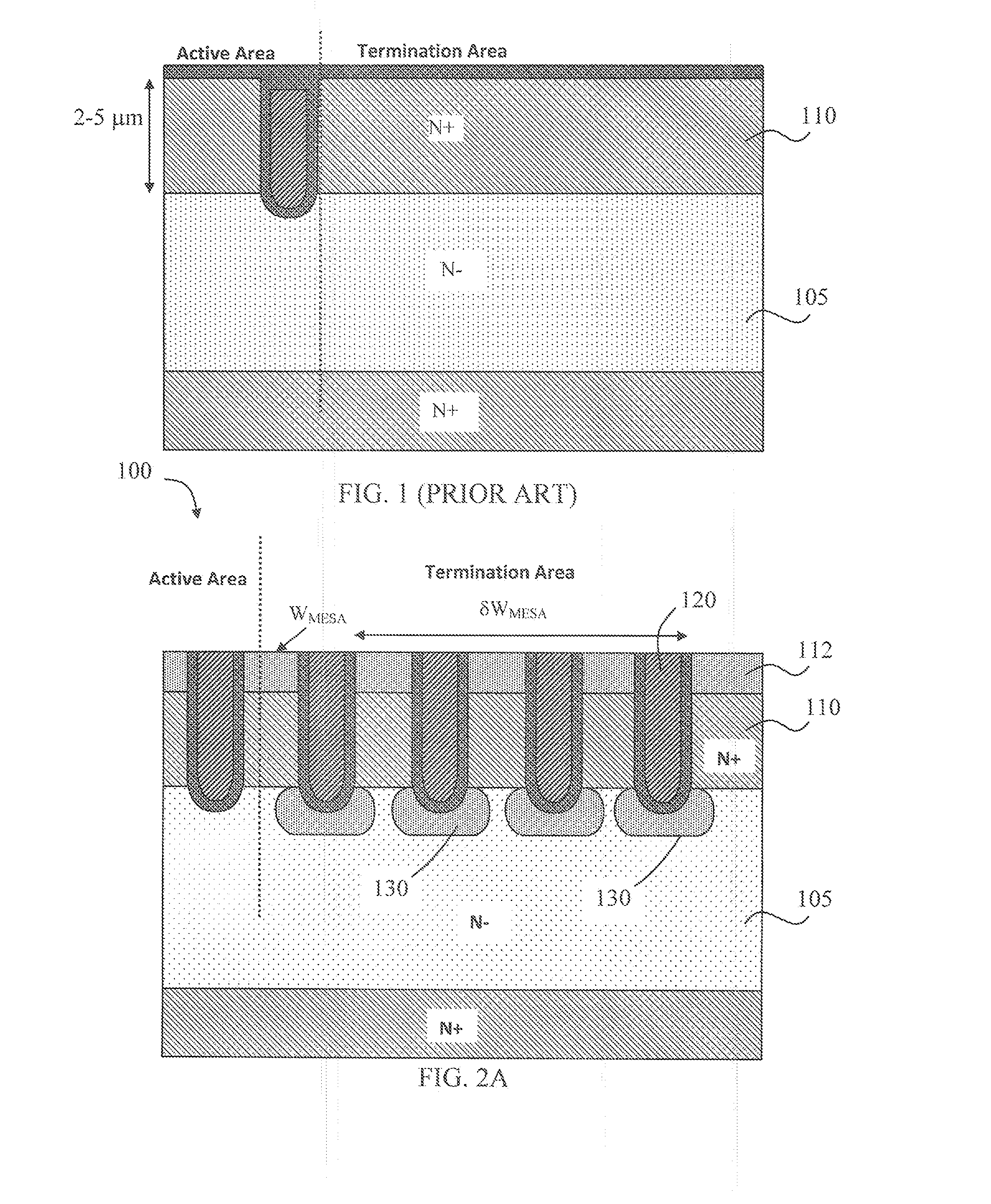
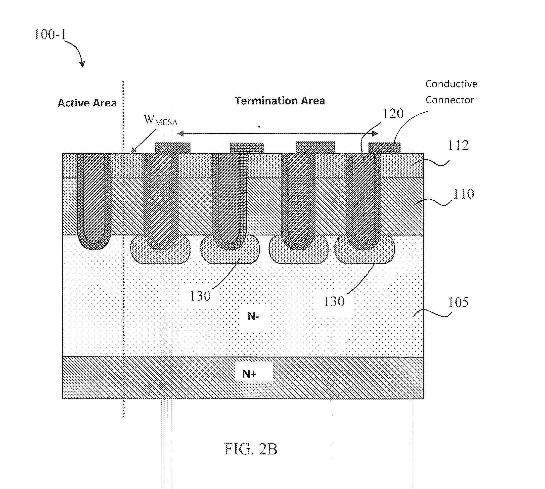
[0018]FIG. 2A is a cross sectional view for illustrating the configuration of an edge termination 100 with buried guard rings of this invention for a high voltage (HV) device that includes a heavily doped N region 110 formed on a lightly doped N-type substrate 105. A P-type body region 112 is also formed at the top of the heavily doped N region 110. The edge termination 100 includes a plurality of edge termination trenches 120 lined with a dielectric layer 125, e.g., oxide layer, on the sidewalls and bottom surface of the trenches and then filled with a conductive material, such as polysilicon. A buried guard ring doped P-type region 130 is formed in the substrate 105 immediately below the bottom surface of each of the edge termination trenches 120. The buried guard ring doped regions 130 are formed by implanting through the edge termination trenches 120 as will be further discussed below. The pinch-off of the buried guard rings 130 limits the voltage drop across the mesa regions, W...


PUM


Abstract

This invention discloses a semiconductor power device disposed in a semiconductor substrate comprising a heavily doped region formed on a lightly doped region and having an active cell area and an edge termination area. The edge termination area comprises a plurality of termination trenches formed in the heavily doped region with the termination trenches lined with a dielectric layer and filled with a conductive material therein. The edge termination further includes a plurality of buried guard rings formed as doped regions in the lightly doped region of the semiconductor substrate immediately adjacent to the termination trenches.

Description

[0001]This Patent Application is a Divisional Application and claim the Priority Date of a co-pending application Ser. No. 13 / 135,982 filed by the Applicants of this Application on Jul. 19, 2011. The Disclosures made in application Ser. No. 13 / 135,982 are hereby incorporated by reference.BACKGROUND OF THE INVENTION[0002]1. Field of the Invention[0003]The invention relates generally to the semiconductor power devices. More particularly, this invention relates to configurations and methods for manufacturing of new and improved edge terminations for high voltage (HV) devices for improved reliability and to reduce the areas occupied by the termination areas while maintaining high breakdown voltages.[0004]2. Description of the Prior Art[0005]Conventional floating guard rings in the termination area are not sufficient to sustain high breakdown voltages for high-voltage (HV) devices that have heavily doped N regions 110, e.g., doping concentration of 1016 dopants / cm3, of about two to five ...

Claims


Application Information

Patent Timeline
Patent Type & Authority Applications(United States)
IPC IPC(8): H01L29/06H01L21/761H01L29/78
CPCH01L29/0623H01L21/761H01L29/7823H01L29/404H01L29/407H01L29/66734H01L29/7813H01L29/7811H01L29/0619
Inventor LEE, YEEHENGBOBDE, MADHURDING, YONGPINGKIM, JONGOHBHALLA, ANUP
Owner LEE YEEHENG
Why Eureka
Try Eureka