Schottky diode structure and method for fabricating the same

a diode and diode technology, applied in the field of schottky diode structure, can solve the problems of poor heat conduction between sapphire and gallium nitride, unfavorable use in high-power applications, and relatively low breakdown voltage of the entire schottky diode, so as to reduce the non-uniform distribution of electric fields and increase the breakdown voltage of the schottky diode

Active Publication Date: 2011-12-22
NATIONAL TSING HUA UNIVERSITY
View PDF4 Cites 5 Cited by
  • Summary
  • Abstract
  • Description
  • Claims
  • Application Information

AI Technical Summary

Benefits of technology

[0007]The primary objective of the present invention is to provide a Schottky diode structure and a method for fabricating the same, which can increase the breakdown voltage of the Schottky diode and decrease the non-uniform distribution of the electric field to prevent from the breakdown of the substrate and the gallium nitride layer of the Schottky diode.

Problems solved by technology

However, the poor heat conduction between sapphire and gallium nitride is unfavorable for use in high power application.
Further, the silicon carbide substrate is expensive and has limited commercial application.
Therefore, too thin an N-type gallium nitride layer is likely to cause the breakdown of the silicon substrate and results in a relatively lower breakdown voltage of the entire Schottky diode.
However, a thicker gallium nitride layer is expensive.
Further, the lattice mismatch between gallium nitride and silicon is very great and likely to generate crystal dislocation and result in poor reliability.

Method used


Image

  • Schottky diode structure and method for fabricating the same
  • Schottky diode structure and method for fabricating the same
  • Schottky diode structure and method for fabricating the same

Examples


Embodiment Construction

[0017]The technical contents of the present invention are described in detail in cooperation with the drawings below.

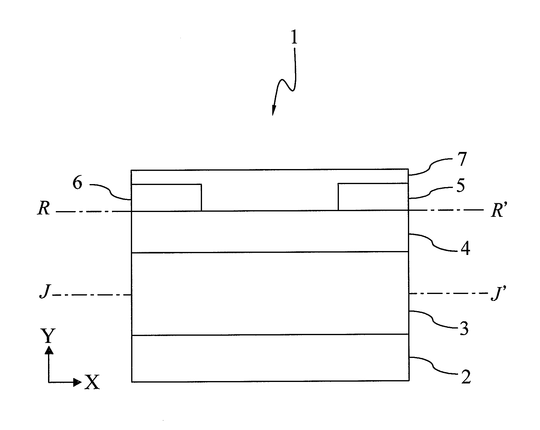
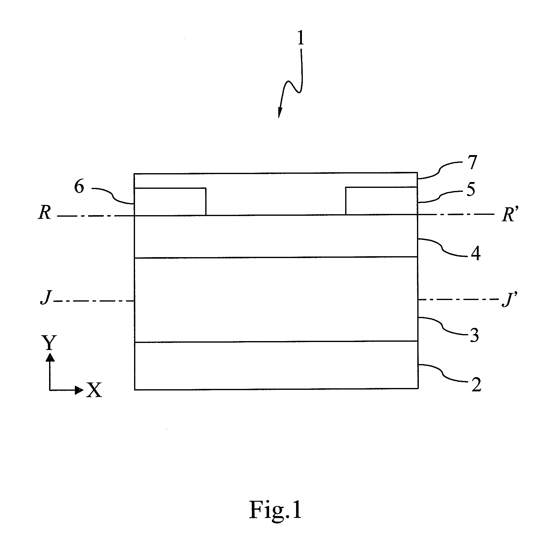
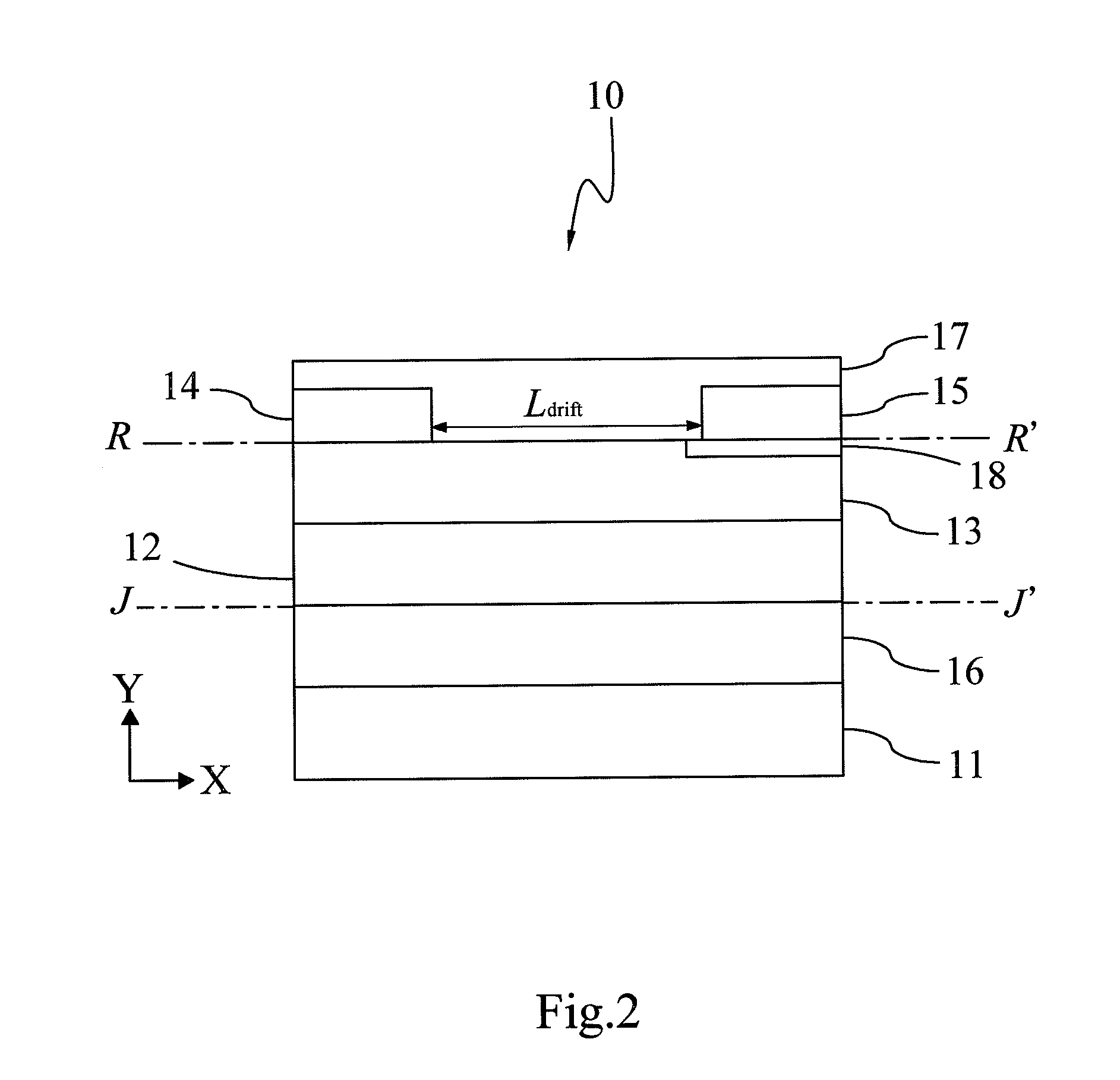
[0018]Refer to FIG. 2 a diagram schematically showing a Schottky diode structure according to one embodiment of the present invention. The Schottky diode structure 10 of the present invention comprises a substrate 11, a P-type gallium nitride layer 12 formed on the substrate 11, an N-type gallium nitride layer 13 formed on the P-type gallium nitride layer 12, a Schottky electrode 14 and an ohmic contact electrode 15 both formed on the N-type gallium nitride layer 13.

[0019]The substrate 11 is made of an appropriate material. The material of the substrate 11 may be but is not limited to a material selected from a group consisting of sapphire (Al2O3), silicon carbide (SiC), silicon (Si), spinel, diamond, diamond like carbon (DLC), aluminum nitride (AlN), lanthanum gallate (LiGaO3), lanthanum aluminate (LiAlO3), zinc oxide (ZnO), gallium nitride (GaN), gallium phosphide (...


PUM

PropertyMeasurementUnit
breakdown voltageaaaaaaaaaa
thicknessaaaaaaaaaa
breakdown voltageaaaaaaaaaa

Abstract

A Schottky diode structure and a method for fabricating the same, which are based on the principle of charge compensation, wherein a P-type gallium nitride layer is added to a Schottky diode structure, and wherein the PN junction of the P-type gallium nitride layer and the N-type gallium nitride layer decreases the non-uniformity of the surface electric field distribution, whereby the breakdown voltage of the element is raised.

Description

FIELD OF THE INVENTION[0001]The present invention relates to a Schottky diode structure and a method for fabricating the same, particularly to a gallium nitride-based Schottky diode structure having a high-breakdown voltage and a method for fabricating the same.BACKGROUND OF THE INVENTION[0002]The Schottky diode is a power rectifier widely applied to many fields, such as power supply devices, power converters, motor controllers, telecommunication switches, factory automation apparatuses, electronic automation devices and low-voltage converters. The Schottky diode is indeed superior in switching speed. However, the Schottky diode still needs careful design in the materials and structures to achieve a low reverse leakage current, a high breakdown voltage and a low turn-on voltage so as to achieve the best performance.[0003]In comparison with the silicon-based Schottky diode, the gallium nitride Schottky diode has a wider energy gap and a better carrier conduction performance. Therefor...

Claims


Application Information

Patent Timeline
Patent Type & Authority Applications(United States)
IPC IPC(8): H01L29/872H01L21/329H01L29/20
CPCH01L29/063H01L29/2003H01L29/872H01L29/861H01L29/475
Inventor HSU, SHUO-HUNGLIAN, YI-WEILIN, YU-SYUAN
Owner NATIONAL TSING HUA UNIVERSITY
Why Eureka
Try Eureka