High aspect ratio plasma etch for 3D NAND semiconductor applications

a plasma etching and high aspect ratio technology, applied in semiconductor devices, electrical equipment, electric discharge tubes, etc., can solve problems such as device failur

Inactive Publication Date: 2016-02-25
APPLIED MATERIALS INC
View PDF0 Cites 17 Cited by
  • Summary
  • Abstract
  • Description
  • Claims
  • Application Information

AI Technical Summary

Benefits of technology

[0011]Embodiments of the present disclosure provide an apparatus and methods for forming high aspect features in a film stack, which may be utilized to form stair-like structures, with accurate profiles and dimension control for manufacturing three dimensional (3D) stacked semiconductor chips. In one example, a method of etching a material layer disposed on a substrate using synchronized RF pulses includes providing an etching gas mixture into a processing chamber having a film stack disposed on a substrate, synchronously pulsing a RF source power and a RF bias power into the etching gas mixture at a ratio of less than 0.5, and etching the film stack disposed on the substrate.
[0012]In another example, a method of etching a film stack disposed on a substrate using synchronized RF pulses includes providing an etching gas mixture into a processing chamber having a film stack disposed on a substrate, wherein the film stack includes repeated pairs of layers, synchronously pulsing a RF source power at a frequency greater than 2.5 MHz and a RF bias power at a frequency less than 2.5 MHz into the etching gas mixture at a ratio of less than 0.5, and etching the film stack disposed on the substrate.
[0013]In yet another example, a method of etching a film stack disposed on a substrate using synchronized RF pulses, the film stack utilized to form a stair-like structures on the substrate includes providing an etching gas mixture including a fluorine-carbon containing and a halogen containing gas into a processing chamber having a film stack disposed on a substrate, wherein the film stack includes repeated pairs of layers, synchronously pulsing a RF source power at a frequency greater than 2.5 MHz and a RF bias power at a frequency less than 2.5 MHz into the etching gas mixture at a ratio of less than 0.5, and etching the film stack disposed on the substrate to form features with aspect ratio greater than 20:1.

Problems solved by technology

Reliably producing sub-half micron and smaller features is one of the key technology challenges for next generation very large scale integration (VLSI) and ultra large-scale integration (ULSI) of semiconductor devices.
However, as the limits of circuit technology are pushed, the shrinking dimensions of VLSI and ULSI interconnect technology have placed additional demands on processing capabilities.
As the geometry and the aspect ratio of the structures become even smaller and higher, the stress mismatch issue occurred between different materials in the film stack become increasingly dominant, thereby resulting in stress induced line edge roughness or line breakage, eventually resulting in device failure.

Method used


Image

  • High aspect ratio plasma etch for 3D NAND semiconductor applications
  • High aspect ratio plasma etch for 3D NAND semiconductor applications
  • High aspect ratio plasma etch for 3D NAND semiconductor applications

Examples


Embodiment Construction

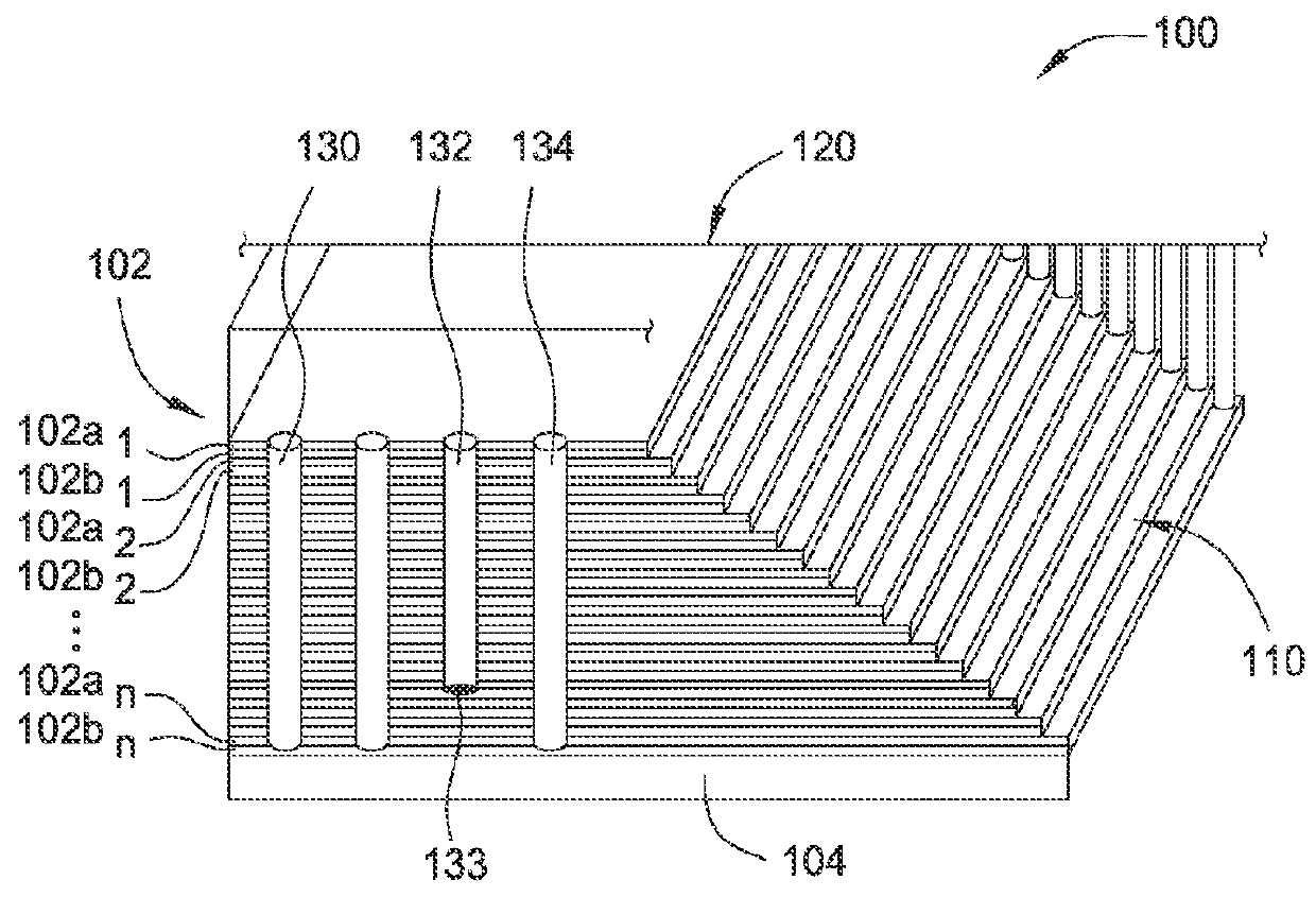
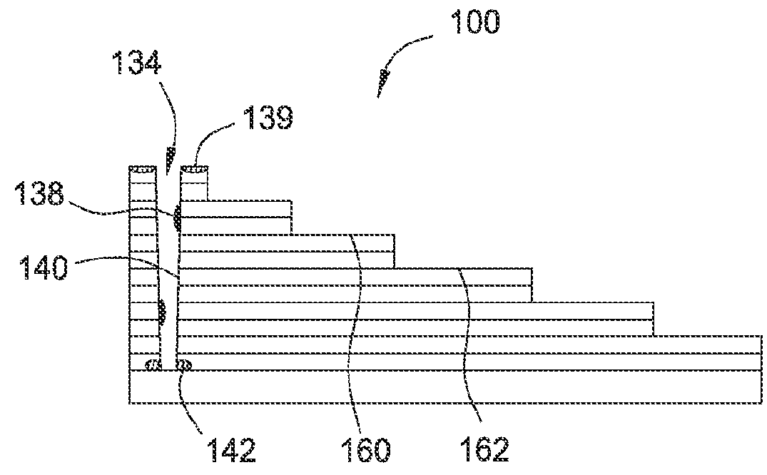
[0022]The present invention provides methods for forming features in a film stack which may be utilized to form stair-like structures on a substrate for three dimensional (3D) stacking of semiconductor chips. In one example, precise dimension control, accurate feature transfer and good process control during etching may be obtained through synchronizing pulses of a RF source power and a RC bias power at a predetermined ratio. By utilizing synchronized pulses of the RF source power and the RC bias power during an etch process, the trajectory of reactive species generated in the plasma may be extended, thus pulling reactive species down to a bottom of the film stack, so as to successfully form features with high aspect ratios in the film stack.

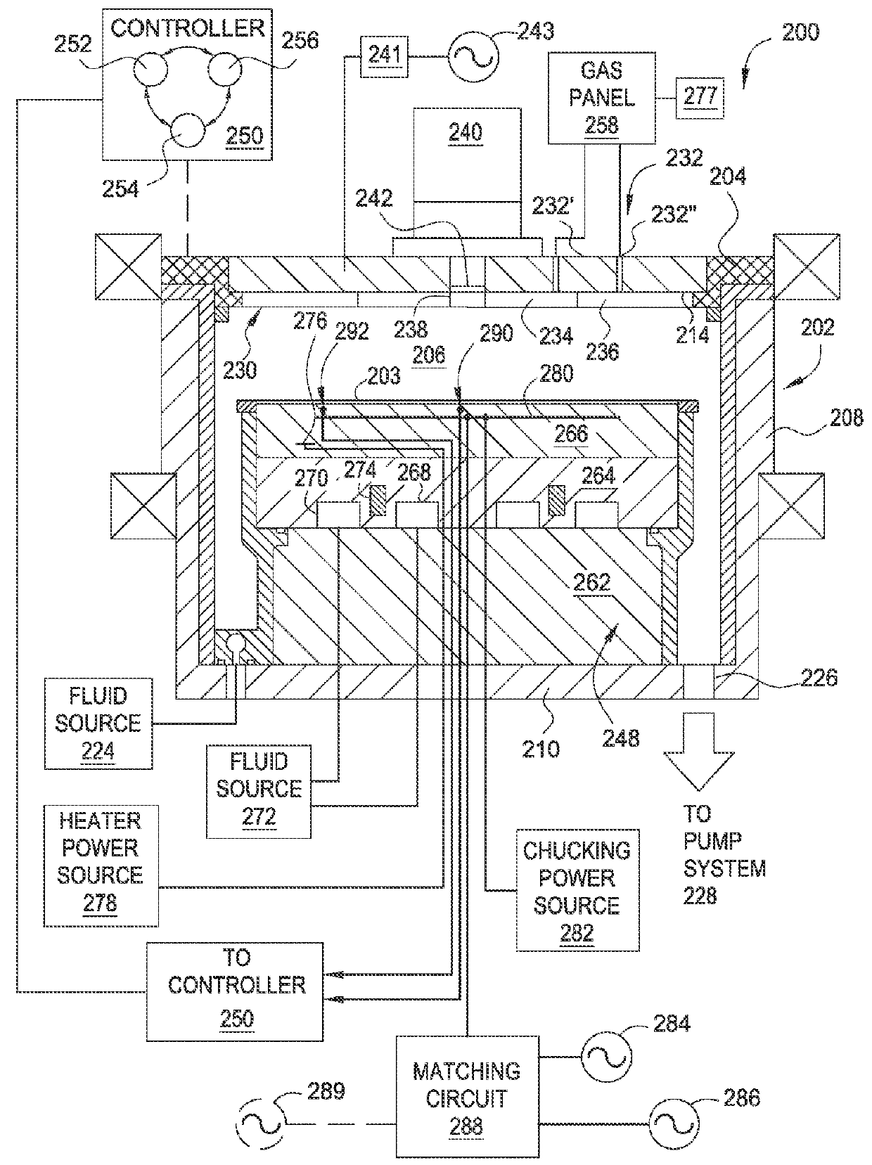
[0023]FIG. 2 is a sectional view of one example of a processing chamber 200 suitable for performing an etch process to form features in a film stack with high aspect ratio, such as greater than 20:1. Suitable processing chambers that may be adap...


PUM


Abstract

Embodiments of the present disclosure provide methods for forming features in a film stack that may be utilized to form stair-like structures with accurate profiles control in manufacturing three dimensional (3D) stacking of semiconductor chips. In one example, a method of etching a material layer disposed on a substrate using synchronized RF pulses includes providing an etching gas mixture into a processing chamber having a film stack disposed on a substrate, synchronously pulsing a RF source power and a RF bias power into the etching gas mixture at a ratio of less than 0.5, and etching the film stack disposed on the substrate.

Description

BACKGROUND[0001]1. Field[0002]Embodiments of the present invention generally relate to methods of forming high aspect ratio features in a vertical type semiconductor device, and more particularly to methods of forming high aspect ratio features in a vertical type semiconductor device with stair-like structures for semiconductor applications.[0003]2. Description of the Related Art[0004]Reliably producing sub-half micron and smaller features is one of the key technology challenges for next generation very large scale integration (VLSI) and ultra large-scale integration (ULSI) of semiconductor devices. However, as the limits of circuit technology are pushed, the shrinking dimensions of VLSI and ULSI interconnect technology have placed additional demands on processing capabilities. Reliable formation of gate structures on the substrate is important to VLSI and ULSI success and to the continued effort to increase circuit density and quality of individual substrates and die.[0005]A patter...

Claims


Application Information

Patent Timeline
Patent Type & Authority Applications(United States)
IPC IPC(8): H01L21/311H01L27/115
CPCH01L21/31116H01L27/11582H01L27/11556H01L21/32137H01J37/32091H01J37/32146H10B41/27H10B43/27
Inventor KONG, BYUNGKOOKLEE, GENEYANG, LIMING
Owner APPLIED MATERIALS INC
Why Eureka
Try Eureka