

Light emitting device and method for producing the same
a technology of light emitting device and light source, which is applied in the direction of semiconductor/solid-state device manufacturing, semiconductor devices, electrical devices, etc., can solve the problems of reduced formability, reduced fluidity of resin materials, brittle molding, etc., and achieve high frontal luminance, high reliability, and high frontal luminance
- Summary
- Abstract
- Description
- Claims
- Application Information
AI Technical Summary
Benefits of technology
Problems solved by technology
Method used
Image

Examples
first embodiment
Light Emitting Device Configuration
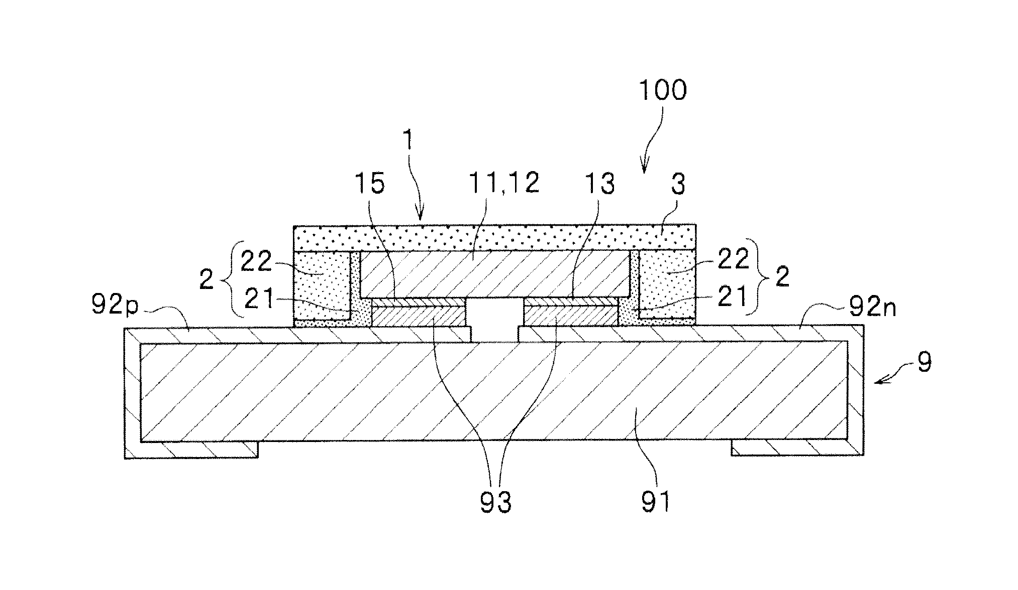
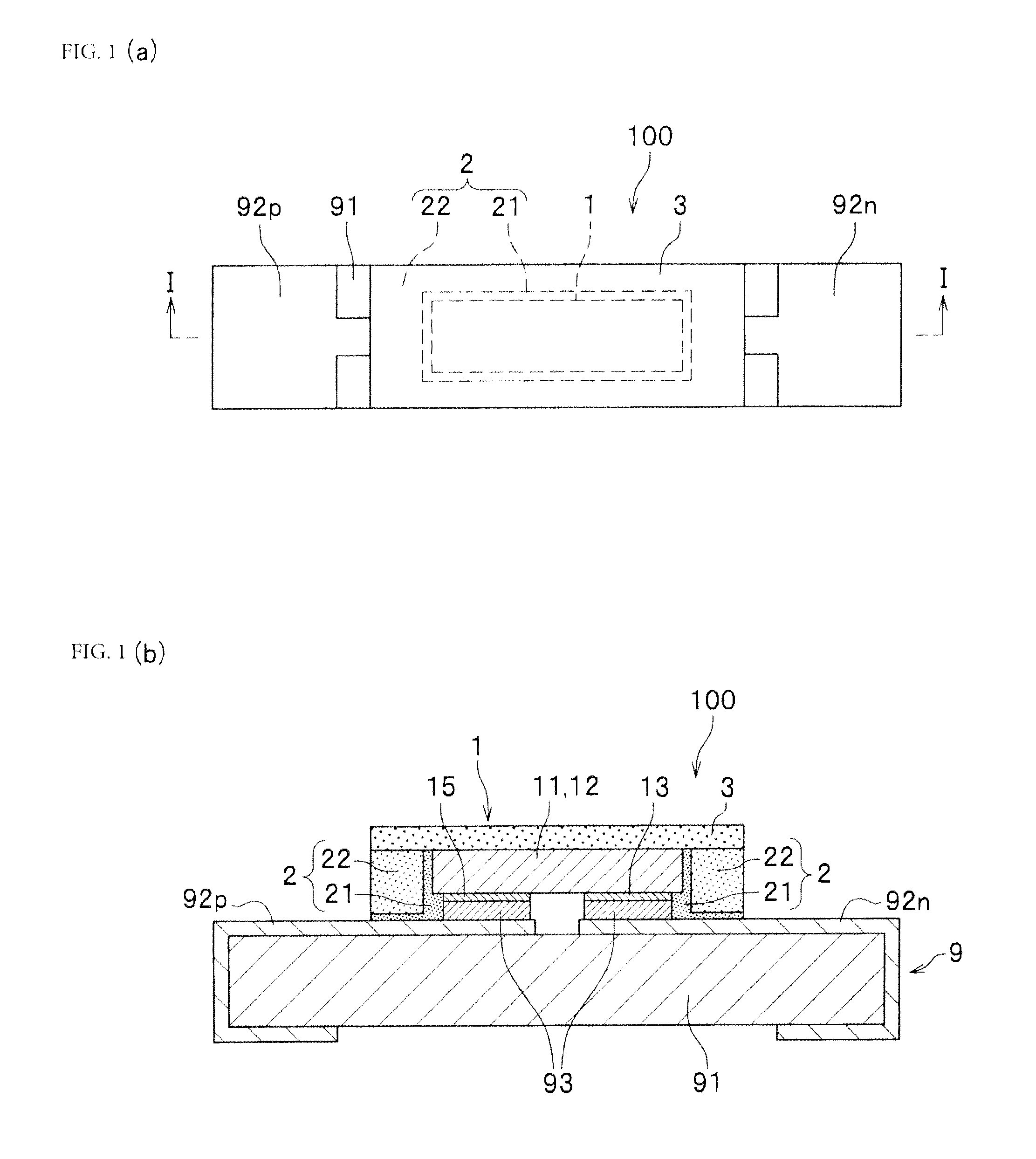
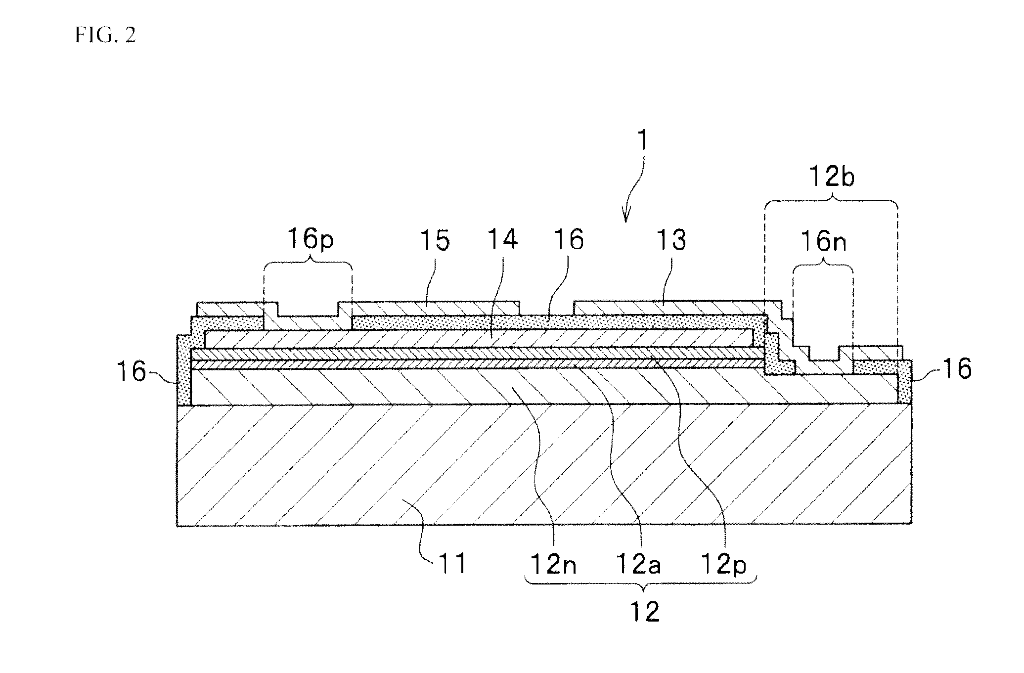
[0040]First, the configuration of the light emitting device according to a first embodiment of the present invention will be explained with reference to FIGS. 1 and 2.
[0041]As shown in FIG. 1, the light emitting device 100 of this embodiment has a semiconductor light emitting element 1 (hereinafter referred to as “light emitting element” when appropriate), a light reflective member 2, a wavelength conversion member 3, and a mounting substrate (submount) 9.
[0042]The light emitting element 1 is flip-chip mounted on a mounting substrate 9 via a conductive adhesive material 93, such as solder.
[0043]On the side faces of the light emitting element 1, a light reflective member 2 having a first layer 21 and second layer 22 is provided to increase the light extraction efficiency from the upper face of the light emitting element 1.
[0044]On the upper face of the light emitting element 1, moreover, a wavelength conversion member 3 is provided to allow at least...
second embodiment
Light Emitting Device Configuration
[0154]Subsequently, the light emitting device according to a second embodiment will be explained with reference to FIG. 9.
[0155]As shown in FIG. 9, the light emitting device 100A according to the second embodiment is different from the light emitting device 100 in the first embodiment shown in FIG. 1 such that the wavelength conversion member 3 is provided only on the upper face of the light emitting element 1; a transparent layer 7 is provided on the upper face of the wavelength conversion member 3; and the light reflective member 2 is provided to the height that covers the side faces of the wavelength conversion member 3 and transparent layer 7.
[0156]In the light emitting device 100A, the wavelength conversion member 3 is provided in the same region as that of the upper face of the light emitting element 1 in a plan view, and its side faces are covered by the light reflective member 2. Thus, the frontal emission luminance (upward direction in FIG...
third embodiment
Light Emitting Device Configuration
[0176]Subsequently, the light emitting device according to a third embodiment will be explained with reference to FIG. 12.
[0177]As illustrated in FIG. 12, the light emitting device 100B according to the third embodiment is different from the light emitting device 100 in the first embodiment shown in FIG. 1 such that it has a light reflective member 2B instead of the light reflective member 2. In the light reflective member 2B, the first layer 21B is provided on the side faces of the light emitting element 1 via a resin rich layer 23.
[0178]The first layer 21B, as in the case of the first layer 21 in the first embodiment, has a high content of light reflective substance. When it has a high content of particles of the light reflective substance (for example, 95 mass % or higher), it might not sufficiently adhere to the light emitting element 1 on occasion. In this embodiment, therefore, a resin rich layer 23 which has a low light reflective substance ...
PUM
 Abstract
Description
Claims
Application Information