Display device and manufacturing method thereof

Inactive Publication Date: 2016-06-09
SAMSUNG DISPLAY CO LTD
View PDF2 Cites 2 Cited by
  • Summary
  • Abstract
  • Description
  • Claims
  • Application Information

AI Technical Summary

Benefits of technology

The present patent is about a display device made using a single substrate, which has advantages such as reduced weight, thickness, cost, and processing time. The method of manufacturing the display device prevents the color filter from sinking and induces lumping of the alignment layers into the connection microcavity by connecting neighboring microcavities in the column direction of each pixel area. This results in improved manufacturing efficiency and reduced costs.

Problems solved by technology

As a result, the display device may be heavy, thick, and expensive.
Furthermore, the manufacturing process time may be long.

Method used


Image

  • Display device and manufacturing method thereof
  • Display device and manufacturing method thereof
  • Display device and manufacturing method thereof

Examples


Embodiment Construction

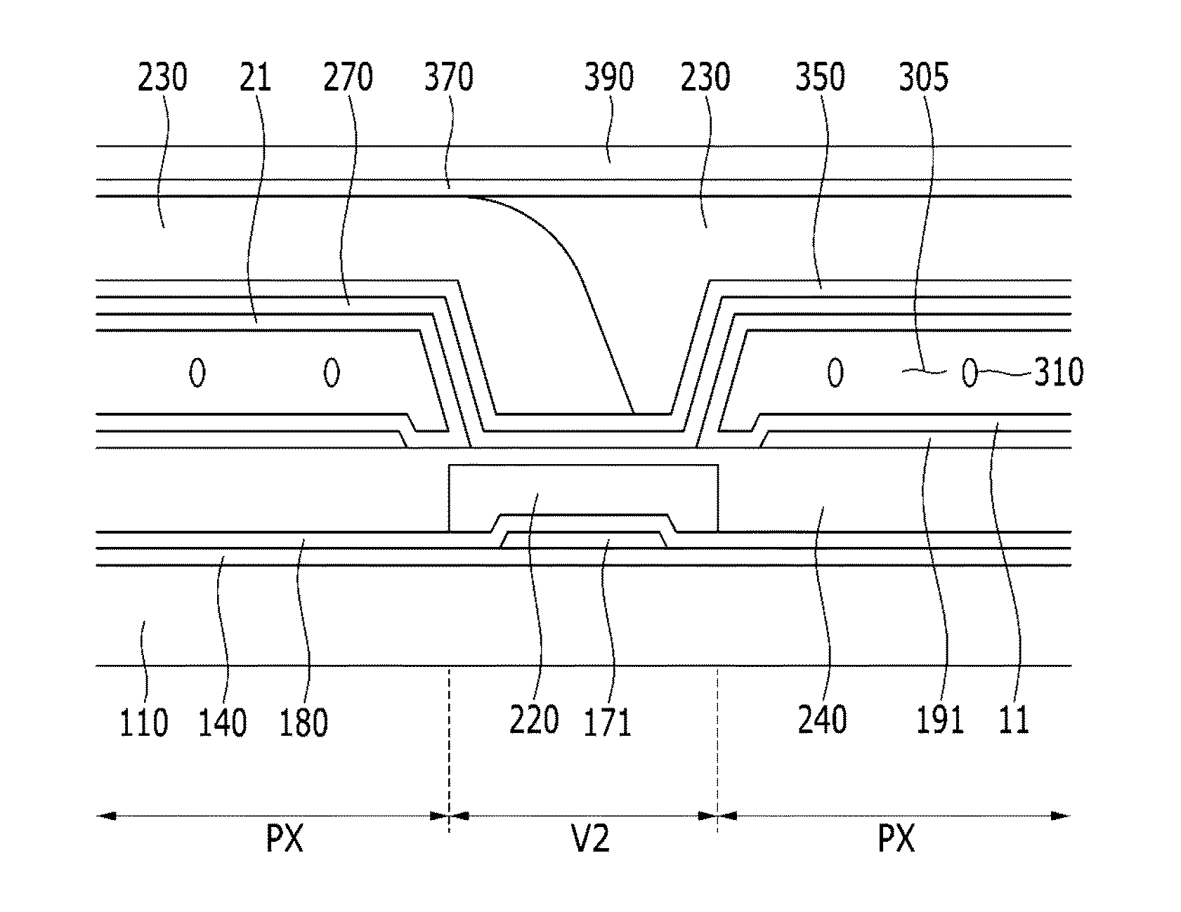
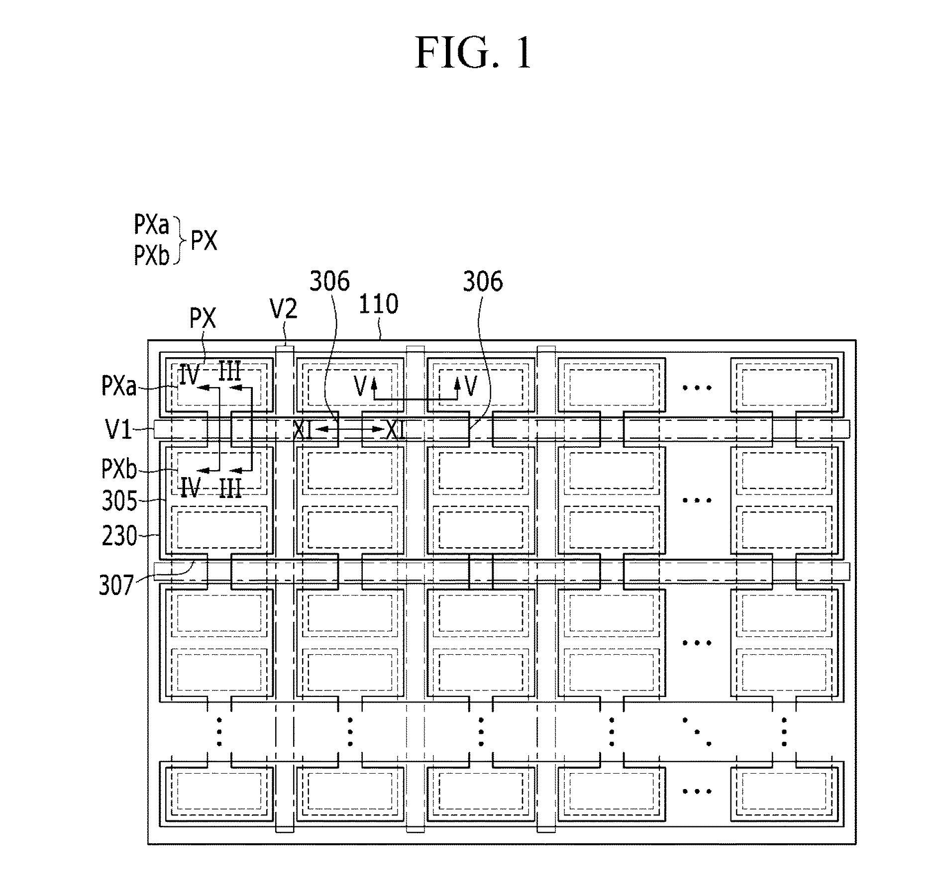
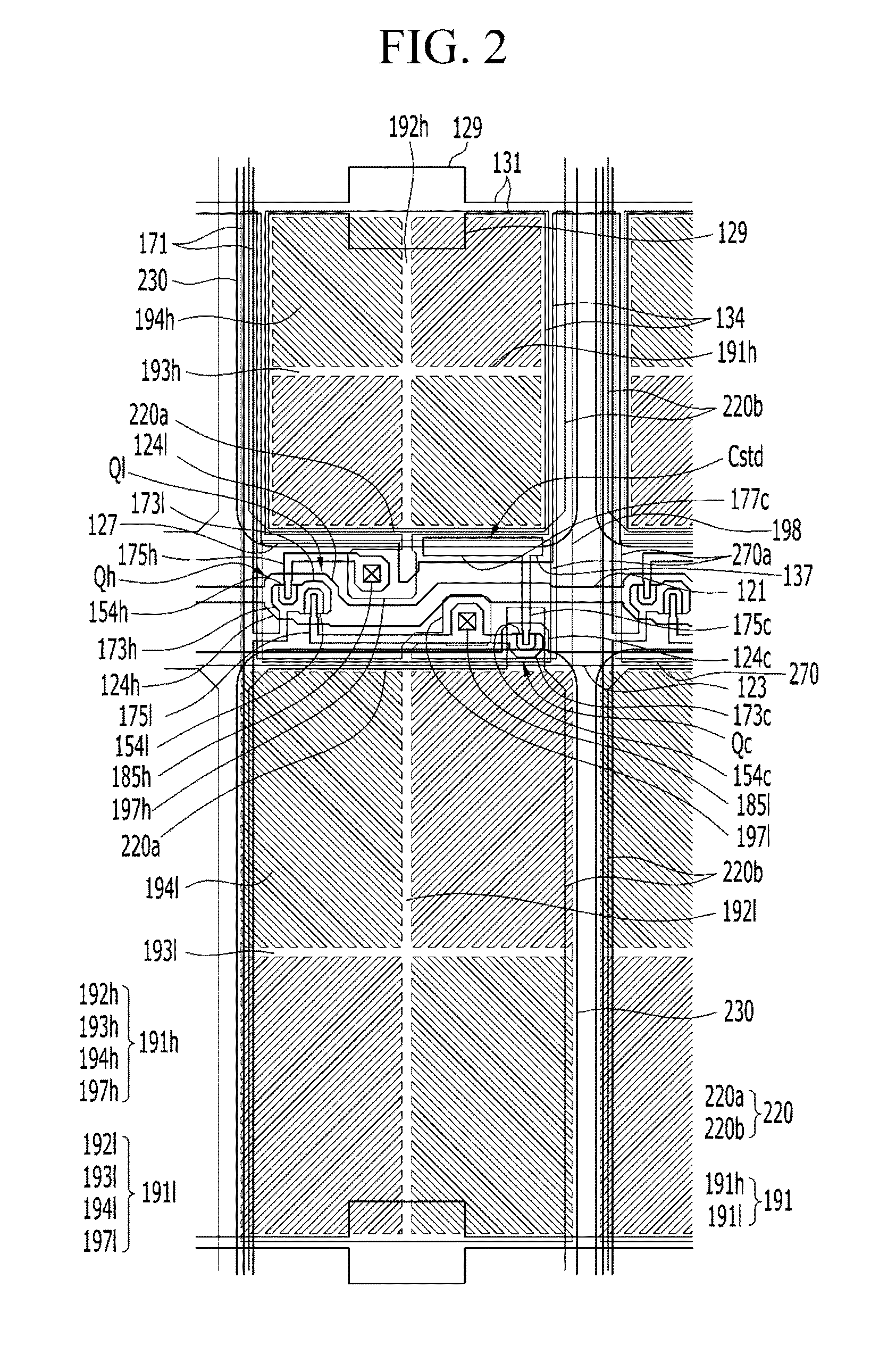
[0046]The present system and method are described with reference to the accompanying drawings in which exemplary embodiments of the present system and method are shown. Those of ordinary skill in the art would realize that the described embodiments may be modified in various different ways without departing from the spirit or scope of the present system and method.

[0047]In the drawings, the thickness of layers, films, panels, regions, etc., are exaggerated for clarity. Like reference numerals designate like elements throughout the specification. When an element such as a layer, film, region, or substrate is referred to as being “on” another element, it can be directly on the other element or intervening elements may also be present. In contrast, when an element is referred to as being “directly on” another element, there are no intervening elements present. Terms indicating directions, positions, and / or orientations of elements generally have the frame of reference of the correspond...


PUM


Abstract

According to an exemplary embodiment of the present system and method, a display device includes: a substrate including a plurality of pixel areas and a thin film transistor region; a plurality of thin film transistors formed on the substrate; a pixel electrode formed in each of the pixel areas and connected to a corresponding thin film transistor; a color filter layer formed on the pixel electrode to be spaced apart from the pixel electrode by a microcavity disposed in between; a plurality of connection microcavities formed in the thin film transistor region and connecting microcavities in a column; and a liquid crystal material filling the microcavities and the connection microcavities.

Description

CROSS-REFERENCE TO RELATED APPLICATION[0001]This application claims priority to and the benefit of Korean Patent Application No. 10-2014-0173325 filed in the Korean Intellectual Property Office on Dec. 4, 2014, the entire contents of which are incorporated herein by reference.BACKGROUND[0002](a) Field[0003]The present disclosure relates to a display device and a manufacturing method thereof.[0004](b) Description of the Related Art[0005]A liquid crystal display generally is a flat panel display and includes two sheets of display panels in which field generating electrodes, such as a pixel electrode and a common electrode, are formed and a liquid crystal layer interposed in between. The liquid crystal display applies a voltage to the field generating electrode to generate an electric field in the liquid crystal layer. The generated electric field determines the orientation of the liquid crystal molecules in the liquid crystal layer, which affects the polarization of incident light of ...

Claims


Application Information

Patent Timeline
IPC IPC(8): G02F1/1333G02F1/1335G02F1/1337G02F1/1368
CPCG02F1/133377G02F1/1368G02F1/1337G02F1/133512G02F1/133516G02F1/133514
Inventor KIM, SI KWANGCHA, TAE WOON
Owner SAMSUNG DISPLAY CO LTD
Why Eureka
Try Eureka