Display device

Inactive Publication Date: 2016-06-09
JAPAN DISPLAY INC
View PDF7 Cites 2 Cited by
  • Summary
  • Abstract
  • Description
  • Claims
  • Application Information

AI Technical Summary

Benefits of technology

The patent text discusses a problem with current display devices where the area of the transistor of the RGB switch cannot be reduced because the current flows through the transistor in a way that makes the channel region larger than the channel length. The technical effect of the patent is to provide a display device that reduces the area of the peripheral region where the transistor is located, by addressing the issue of the large current flow and promoting a more efficient layout.

Problems solved by technology

In such a case, the lengthwise dimension of the peripheral region of the display region in the direction of extension of the signal line becomes large, and the area of the peripheral region of the display region cannot be reduced.

Method used


Image

  • Display device
  • Display device
  • Display device

Examples


first embodiment

[0044]

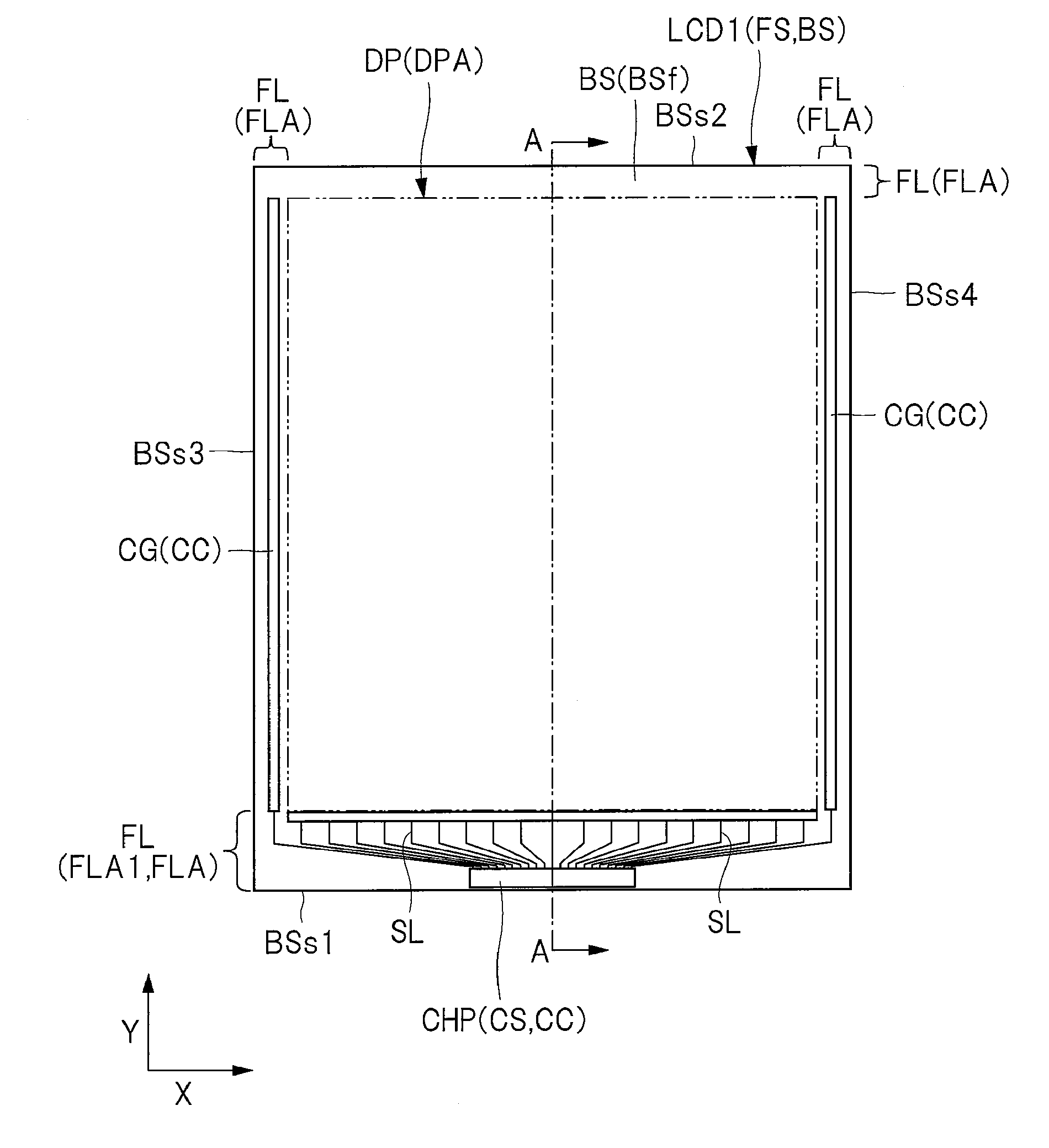
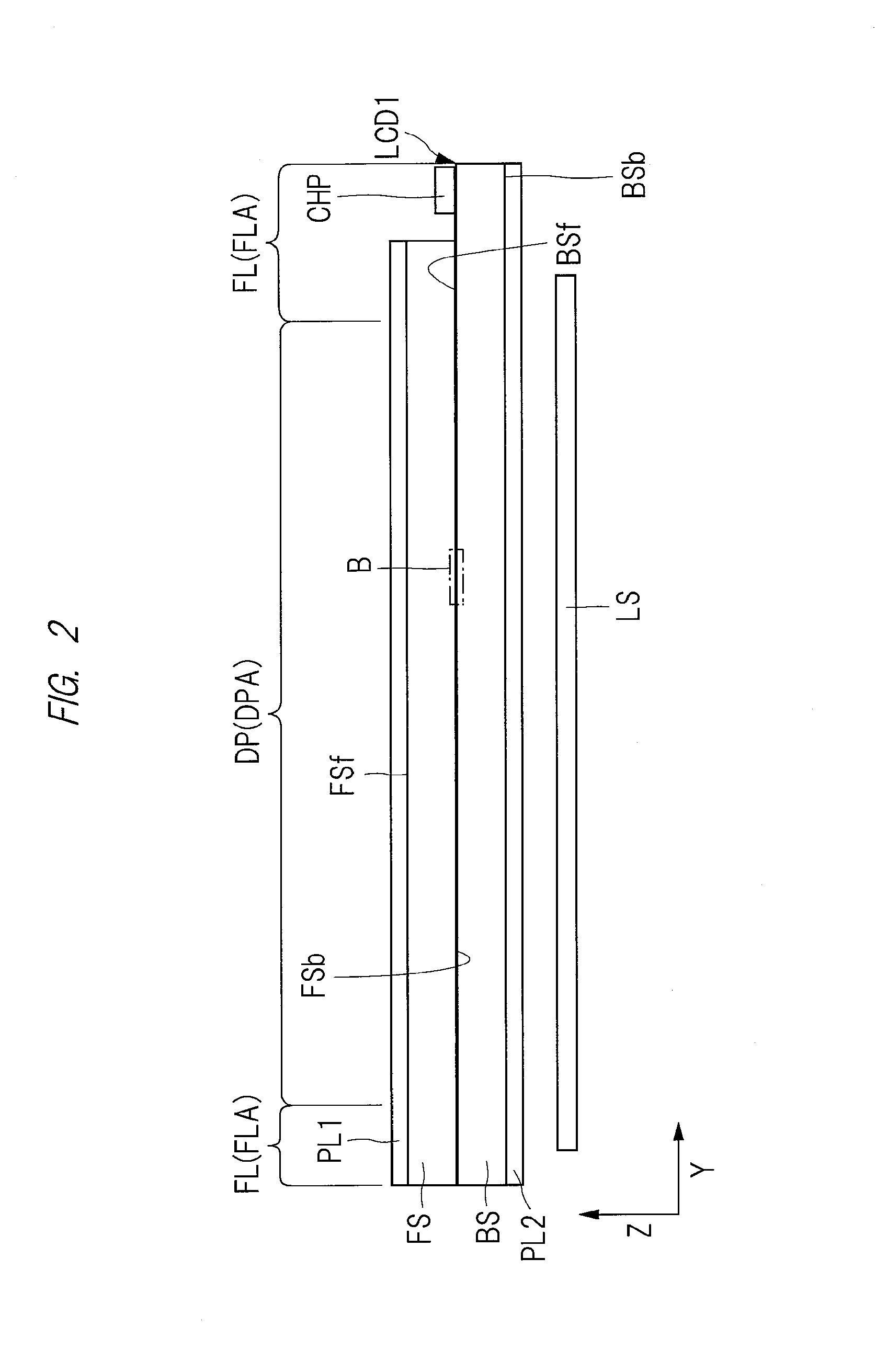
[0045]First, a configuration of the display device will be described. FIG. 1 is a plan view of an example of a display device according to a first embodiment. FIGS. 2 and 3 are cross-sectional views illustrating the example of the display device according to the first embodiment. FIG. 2 is a cross-sectional view taken along a line A-A of FIG. 1. FIG. 3 is an enlarged cross-sectional view of a “B” portion of FIG. 2.

[0046]Note that in FIG. 1, in order to easily see the boundary between a display region DPA and a frame region (peripheral region) FLA when seen in a plan view, the outline of the display region DPA is illustrated by a two-dot chain line. A plurality of video signal lines SL illustrated in FIG. 1 extend from the frame region FLA to the display region DPA. However, in order to easily see FIG. 1, illustration of the video signal lines SL are omitted in the display region DPA. Although FIG. 2 illustrates a cross section, hatching is omitted in order to easily see FIG. 2...

second embodiment

[0144]In the first embodiment, the transistor Tr1 has the extending portion EX11 extending in the direction tilted with respect to the Y direction. On the other hand, in a second embodiment, the transistor Tr1 also has an extending portion EX12 bent and extending from an end of the extending portion EX11 in addition to the extending portion EX11.

[0145]Also in the second embodiment, a configuration and an equivalent circuit of the display device are the same as those of the first embodiment, and explanation for them is omitted.

[0146]

[0147]Next, arrangement of the signal lines and transistors will be described. FIG. 13 is a plan view of the signal lines and transistors according to the second embodiment.

[0148]Note that an equivalent circuit of the signal lines and transistors of the present second embodiment is the same as the equivalent circuit illustrated in FIG. 5. A cross-sectional structure taken along a C-C line of FIG. 13 is the same as the cross-sectional structure illustrated...


PUM


Abstract

An area of a part of a peripheral region of a display region, where a transistor of an RGB switch is provided, is reduced, so that the area of the peripheral region of the display region is reduced. A display device includes a plurality of video signal lines. Each of the plurality of video signal lines has a first signal line connected to a first sub-pixel, a second signal line connected to a second sub-pixel, a first transistor connecting the first signal line to a signal line drive circuit, and a second transistor connecting the second signal line to the signal line drive circuit. Each of the first and second signal lines extends in the Y direction when seen in a plan view, and the first transistor includes an extending portion extending in a direction tilted with respect to the Y direction.

Description

CROSS-REFERENCE TO RELATED APPLICATION[0001]The present application claims priority from Japanese Patent Application No. 2014-246689 filed on Dec. 5, 2014, the content of which is hereby incorporated by reference into this application.TECHNICAL FIELD OF THE INVENTION[0002]The present invention relates to a display device. For example, the present invention relates to a technique effectively applied to a display device having video signal lines for supplying signals to a plurality of pixels arranged in a display region.BACKGROUND OF THE INVENTION[0003]A display device displaying an image by supplying signals to a plurality of pixels arranged in a display region through a plurality of video signal lines is known. In such a display device, it is required to reduce an area of a peripheral region of the display region in order to downsize the display device and make the display region large.[0004]Each of the plurality of pixels includes a plurality of sub-pixels that display each color o...

Claims


Application Information

Patent Timeline
IPC IPC(8): G09G3/36G09G3/20
CPCG09G3/3607G09G2300/0404G09G3/2003G09G3/3648G09G2300/0426G09G2310/0297G02F1/1345
Inventor ISHIGE, NOBUYUKI
Owner JAPAN DISPLAY INC
Why Eureka
Try Eureka