Semiconductor device and method for manufacturing the semiconductor device

Active Publication Date: 2016-06-09
FUJI ELECTRIC CO LTD
View PDF3 Cites 4 Cited by
  • Summary
  • Abstract
  • Description
  • Claims
  • Application Information

AI Technical Summary

Benefits of technology

[0008]The present invention has been made by focusing on such a problem as described above, and it is an object of the present invention to provide a semiconductor device capable of suppressing the deterioration

Problems solved by technology

In an event of wire bonding a metallic wire and a surface of a metallic electrode layer by bringing the metallic wire in contact with the metallic electrode layer, a damage such as a crack sometimes occurs in the electrode layer owing to power of ultrasonic waves

Method used


Image

  • Semiconductor device and method for manufacturing the semiconductor device
  • Semiconductor device and method for manufacturing the semiconductor device
  • Semiconductor device and method for manufacturing the semiconductor device

Examples


Embodiment Construction

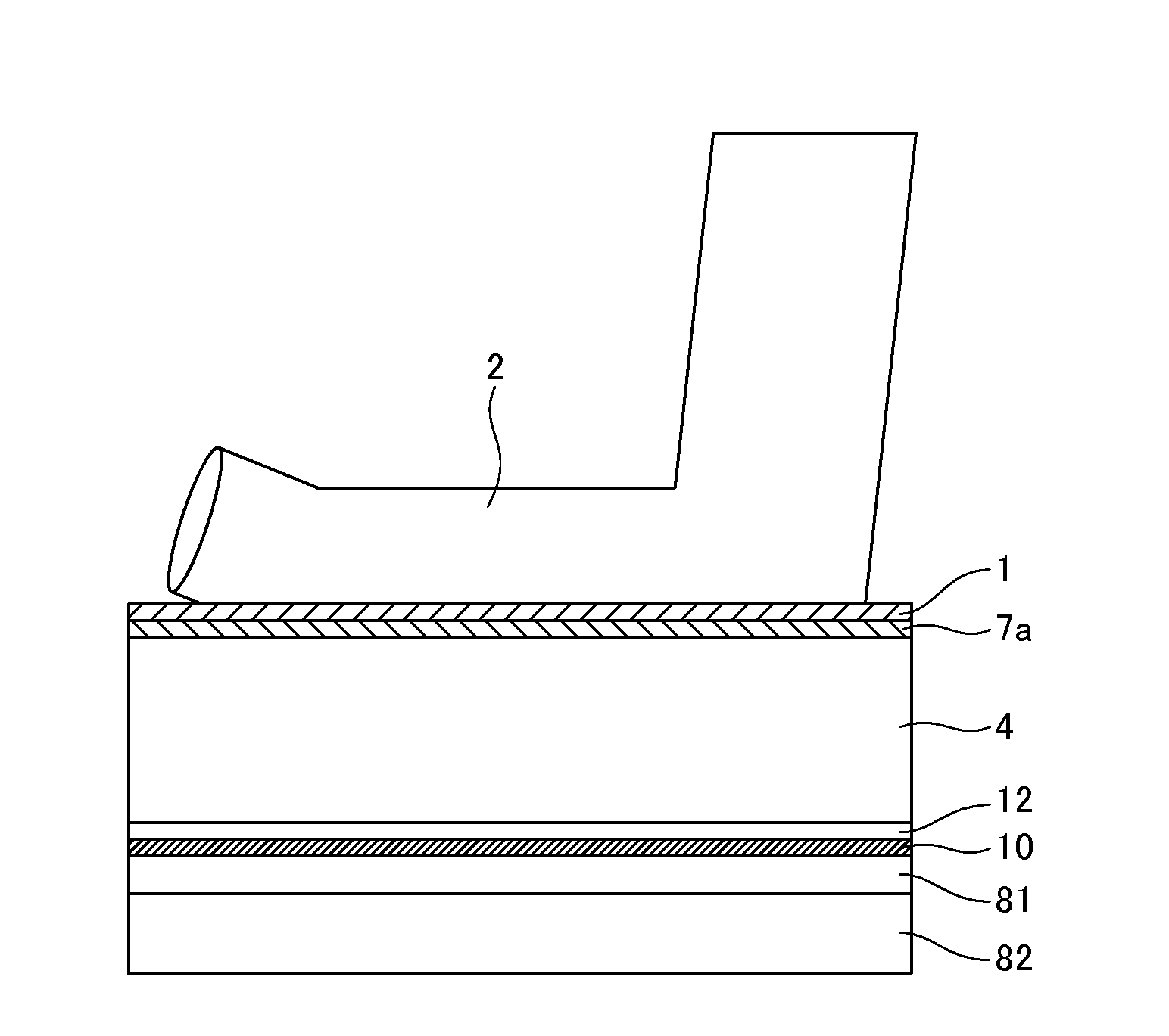
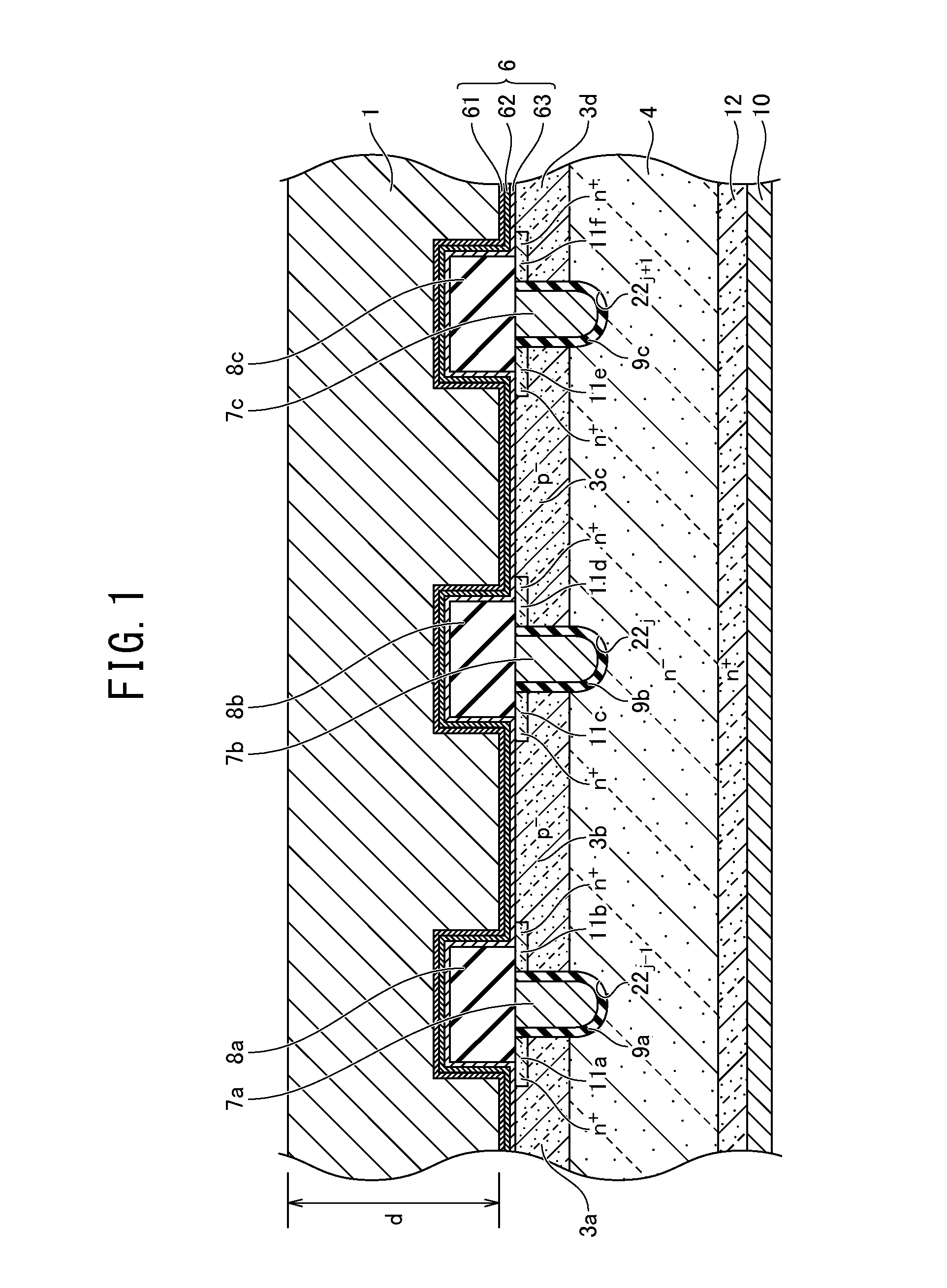
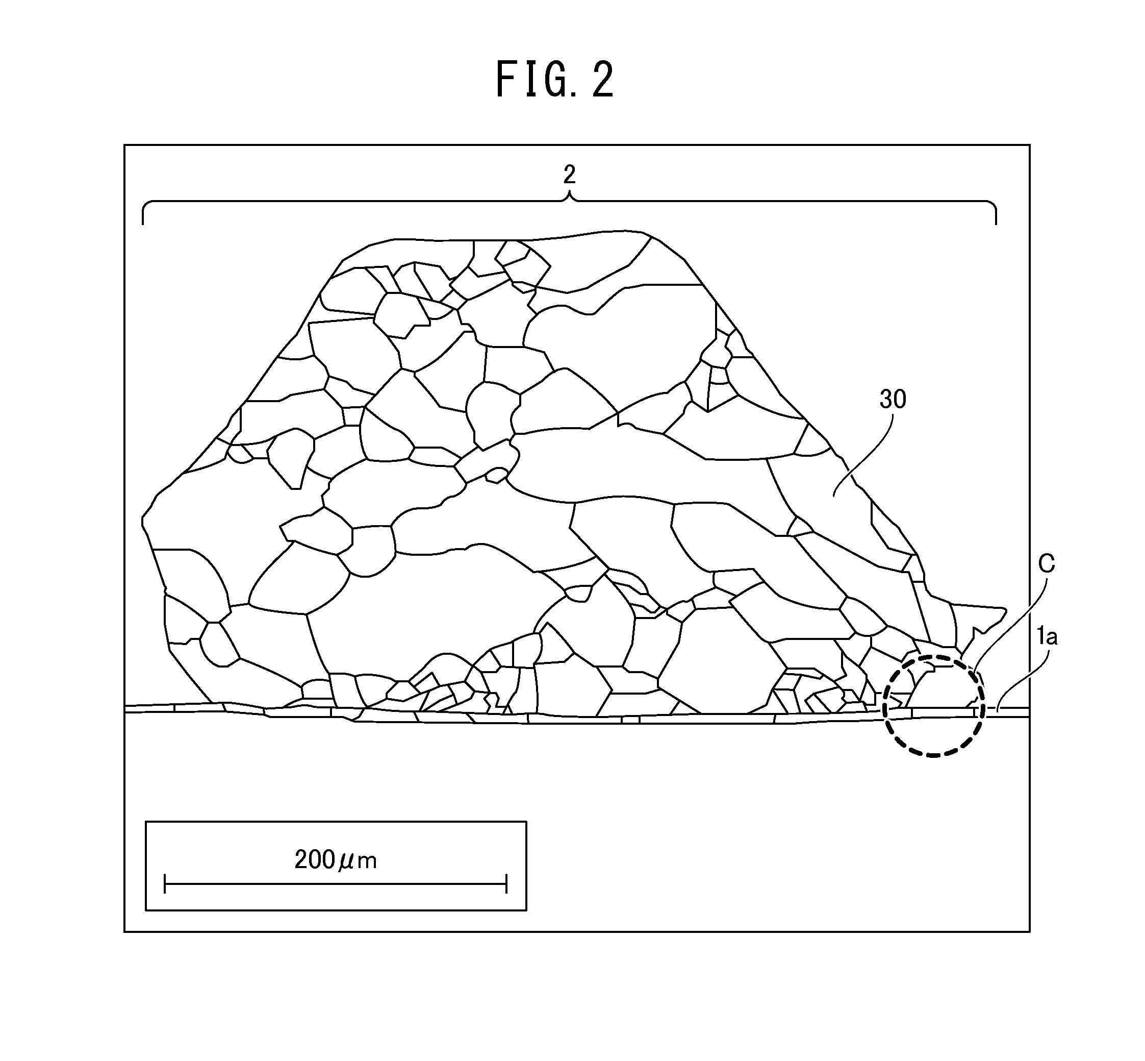
[0018]A description is made below of embodiments of the present invention. In the following description referring to the drawings, the same or similar numerals are assigned to the same or similar portions. However, the drawings are schematic, and it should be noted that a relationship between a thickness and a planar dimension, a thickness ratio of each layer and a wire, and the like are different from actual ones. Hence, specific thickness and dimension should be determined in consideration of the following description. Moreover, as a matter of course, portions different in mutual dimensional relationships and ratios are incorporated also among the drawings. Furthermore, “right and left (crosswise)” and “up and down (vertical)” directions in the following description are merely definitions for convenience of explanation, and do not limit the technical idea of the present invention. Hence, for example, if a space of each of the drawings is rotated by 90 degrees, then “crosswise” and...


PUM


Abstract

A deterioration of a gate threshold voltage, which is caused by a stress and a thermal hysteresis when wire bonding for a surface of an electrode layer of a semiconductor device is performed, can be suppressed. The semiconductor device includes a metallic film provided at a surface of a semiconductor chip, and a wire bonded to an upper surface of the metallic film. The metallic film has a plurality of grains, particle diameters of the grains are substantially equal to or more than a thickness of the metallic film.

Description

CROSS REFERENCE TO RELATED APPLICATIONS AND INCORPORATION BY REFERENCE[0001]This application claims benefit of priority under 35 USC 119 based on Japanese Patent No. P2014-245948 filed Dec. 4, 2014, the entire contents of which are incorporated by reference herein.BACKGROUND OF THE INVENTION[0002]1. Field of the Invention[0003]The present invention relates to a semiconductor device and a method for manufacturing the semiconductor device.[0004]2. Description of the Related Art[0005]For manufacturing semiconductor devices exemplified by diodes, integrated circuits (ICs) and the like, processes for connecting chip-like semiconductor devices, which are diced into a predetermined size from a wafer, to a fixing member such as a lead frame by soldering and the like, and then firmly adhering electrode layers, which are formed on upper surfaces of such semiconductor chips, and electrode terminals of the lead frame to each other by wire bonding, are executed.[0006]In an event of wire bonding ...

Claims


Application Information

Patent Timeline
IPC IPC(8): H01L29/417H01L29/10H01L23/00H01L29/78
CPCH01L29/41741H01L29/7813H01L2924/3512H01L24/48H01L2224/48455H01L29/1095H01L24/03H01L24/06H01L2224/03H01L2224/065H01L2224/45015H01L2224/45124H01L2924/00014H01L24/45H01L2224/4847H01L29/417H01L24/05H01L29/66348H01L29/66356H01L24/85H01L29/7392H01L29/7397H01L2224/05083H01L2224/05166H01L2224/05171H01L2224/0518H01L2224/05184H01L2224/05559H01L2224/05624H01L2224/85205H01L2924/13055H01L2924/13091H01L2924/01028H01L2924/2076H01L2924/01014H01L2924/01029H01L2924/01012H01L2924/0103H01L2924/013H01L2924/01008H01L2924/00H01L24/04
Inventor NISHIMURA, TAKEYOSHI
Owner FUJI ELECTRIC CO LTD
Why Eureka
Try Eureka