Array substrate and display device

a display device and substrate technology, applied in the field of display, can solve the problems of inability to detect undesirable phenomenon, and frequent remnant of transparent electrode, and achieve the effect of eliminating the problem of short circuit of transparent electrod

Inactive Publication Date: 2016-08-25
TCL CHINA STAR OPTOELECTRONICS TECH CO LTD
View PDF6 Cites 3 Cited by
  • Summary
  • Abstract
  • Description
  • Claims
  • Application Information

AI Technical Summary

Benefits of technology

[0008]The present disclosure aims to provide an array substrate and a display device, so that the technical problem of short circuit of transparent electrode can be eliminated promptly.
[0019]The present disclosure has the following beneficial effects. In the array substrate according to the present disclosure, the primary pixel electrode, secondary pixel electrode, and the common terminal electrode of the voltage dividing capacitor of the pixel unit are located at the same patterning layer. If remnant of transparent electrode occurs, the common terminal electrode and the primary pixel electrode (or secondary pixel electrode) would short out. In this case, the potential on the primary pixel electrode (or secondary pixel electrode) is always the same with the common voltage, causing dark spots to be presented on the pixel unit.
[0020]When the display device is detected through the existing detection method, dark spots would still occur to the pixel unit. However, the dark spots can be detected easily, and thus the problem of short circuit of the transparent electrode can be determined and eliminated timely. Therefore, the yield of the product can be improved.

Problems solved by technology

During the manufacturing of liquid crystal display devices, the problem of remnant of transparent electrode would often occur.
Consequently, the brightness of the secondary pixel region is always the same as the primary pixel region, resulting in undesirable phenomenon, such as bright spots on the pixel unit.
In this case, short circuit of transparent electrode would not be able to be detected.
Therefore, in the prior art, the problem of short circuit of transparent electrode can neither be detected timely, nor eliminated promptly.

Method used


Image

  • Array substrate and display device
  • Array substrate and display device
  • Array substrate and display device

Examples


Embodiment Construction

[0028]The present disclosure will be explained in details with reference to the embodiments and the accompanying drawings, whereby it can be fully understood how to solve the technical problem by the technical means according to the present disclosure and achieve the technical effects thereof, and thus the technical solution according to the present disclosure can be implemented. It is important to note that as long as there is no structural conflict, all the technical features mentioned in all the embodiments may be combined together in any manner, and the technical solutions obtained in this manner all fall within the scope of the present disclosure.

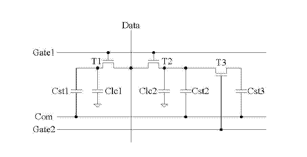
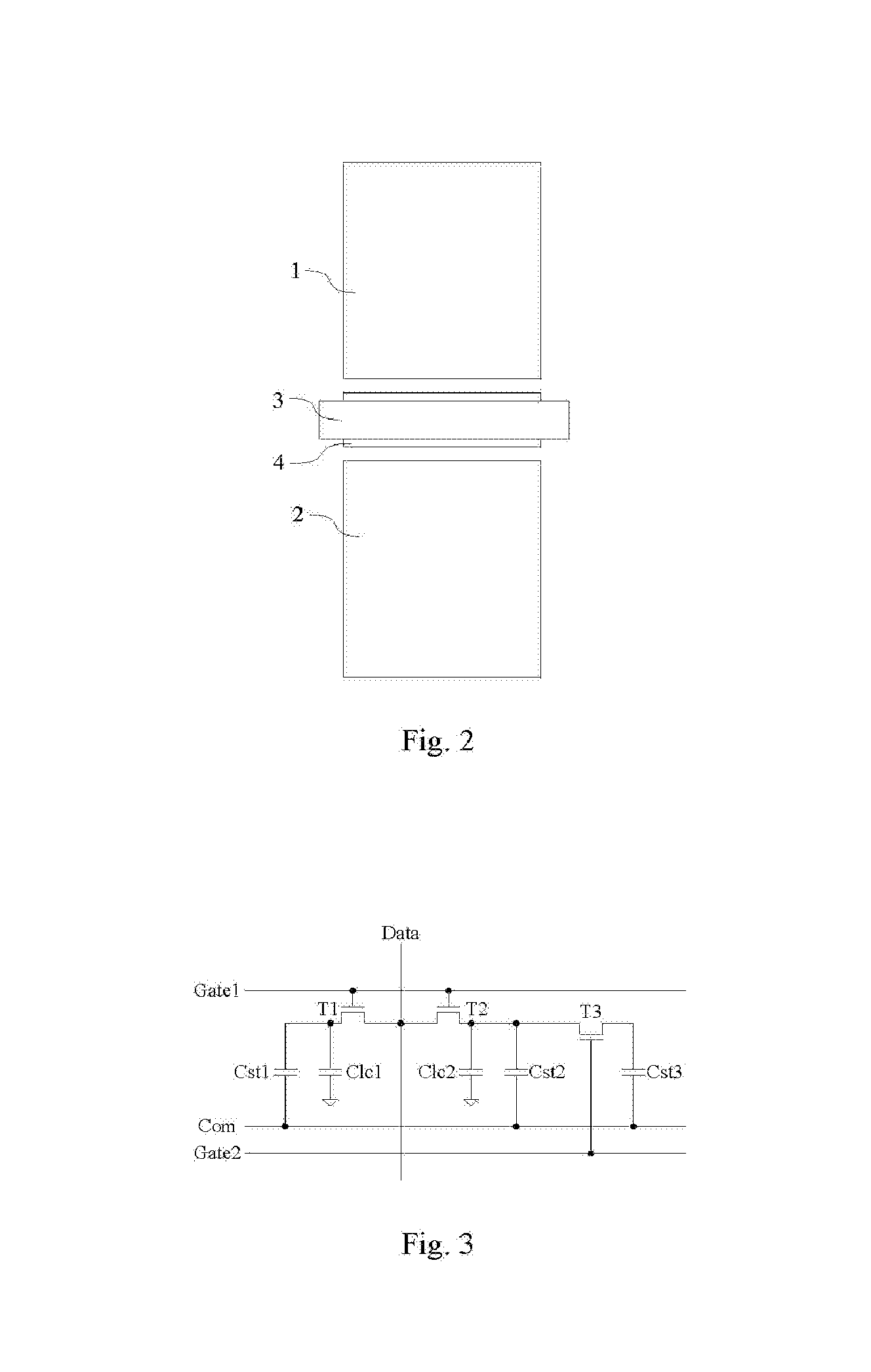
[0029]The present disclosure provides an array substrate which can be used in a vertical alignment liquid crystal display device. The array substrate comprises a plurality of pixel units, each having a primary pixel region, a secondary pixel region, and a voltage dividing capacitor.

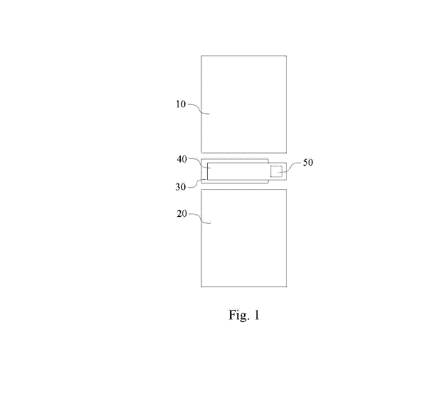
[0030]As shown in FIG. 2, a primary pixel electrode 1 ...


PUM

PropertyMeasurementUnit
voltageaaaaaaaaaa
brightnessaaaaaaaaaa
angleaaaaaaaaaa

Abstract

An array substrate and a display device, which can solve the technical problem of short circuit of transparent electrode and the failure of detection thereof, are provided. In the array substrate, each pixel unit comprises a primary pixel electrode, a secondary pixel electrode, and a voltage dividing capacitor. The voltage dividing capacitor comprises a common terminal electrode and a voltage dividing terminal electrode. The primary pixel electrode, the secondary pixel electrode, and the common terminal electrode are located at the same layer.

Description

[0001]The present application claims benefit of Chinese patent application CN 201410752841.8, entitled “An Array Substrate and A Display Device” and filed on Dec. 10, 2014, the entirety of which is incorporated herein by reference.TECHNICAL FIELD[0002]The present disclosure relates to the technical field of display, and in particular to an array substrate and a display device.TECHNICAL BACKGROUND[0003]As display technology develops, liquid crystal display devices have become the most popular display devices.[0004]A vertical alignment (VA) liquid crystal display device is a common liquid crystal display device. At present, in order to eliminate the phenomenon of color cast with large viewing angle of a VA liquid crystal display device, each pixel unit is divided into a primary pixel region and a secondary pixel region, and further provided with a voltage dividing capacitor therein. As shown in FIG. 1, a primary pixel electrode 10 is disposed in the primary pixel region, a secondary p...

Claims


Application Information

Patent Timeline
Patent Type & Authority Applications(United States)
IPC IPC(8): G02F1/1343H01L27/12G02F1/1333G02F1/1362G02F1/1335G02F1/1368
CPCG02F1/13G02F1/1343G02F1/133345G02F1/1368H01L27/124G02F1/13624G02F1/13439G02F1/134309G02F1/133514G02F1/136286G02F1/1362H01L27/1255G02F1/134345
Inventor WANG, ZUI
Owner TCL CHINA STAR OPTOELECTRONICS TECH CO LTD
Why Eureka
Try Eureka