
Gate-tunable atomically-thin memristors and methods for preparing same and applications of same

a technology of atomically thin memristors and gates, applied in the field of memristors, can solve the problems of lack of control, limited, state-of-the-art memristors based on metal-insulator-metal (mim) structures, etc., and achieve the effect of easily and repeatedly modulating the resistance of grain boundaries emerging from contacts

Active Publication Date: 2016-08-25
NORTHWESTERN UNIV
View PDF0 Cites 30 Cited by
  • Summary
  • Abstract
  • Description
  • Claims
  • Application Information

AI Technical Summary

Benefits of technology

This patent is about a new type of memory device that uses grain boundaries in thin films. The resistance of these boundaries can be easily and repeatedly modulated, and they can produce large changes in resistance levels. This makes them useful for creating new functions in devices. The thin film nature of the device also allows for the tuning of the memory's voltage levels, which is not possible in other types of memories.

Problems solved by technology

State-of-the-art memristors, based on metal-insulator-metal (MIM) structures with insulating oxides such as TiO2, are limited by a lack of control over filament formation and external control of switching voltage [3, 4, 6, 8, 9].
Therefore, a heretofore unaddressed need exists in the art to address the aforementioned deficiencies and inadequacies.

Method used


Image

  • Gate-tunable atomically-thin memristors and methods for preparing same and applications of same
  • Gate-tunable atomically-thin memristors and methods for preparing same and applications of same
  • Gate-tunable atomically-thin memristors and methods for preparing same and applications of same

Examples


Embodiment Construction

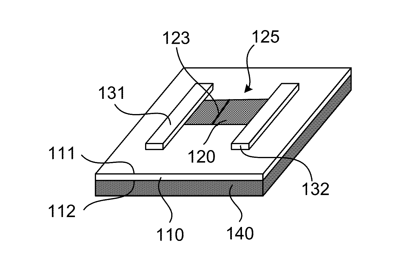
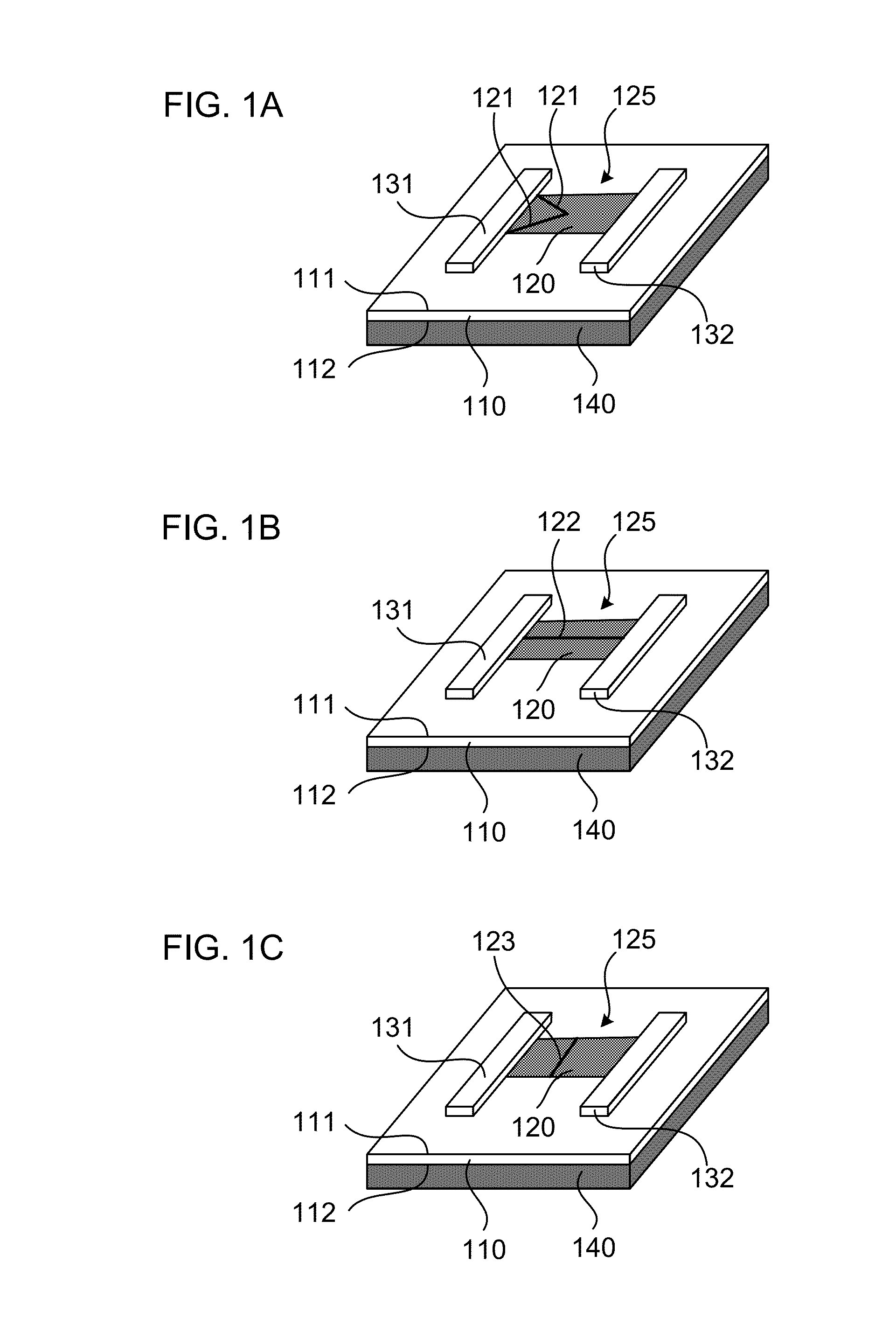
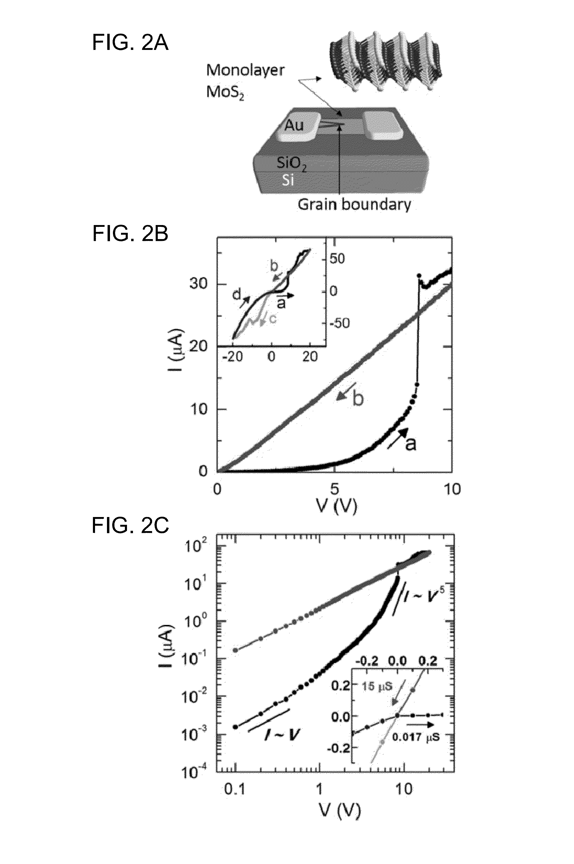
[0066]The invention will now be described more fully hereinafter with reference to the accompanying drawings, in which exemplary embodiments of the invention are shown. This invention may, however, be embodied in many different forms and should not be construed as limited to the embodiments set forth herein. Rather, these embodiments are provided so that this disclosure will be thorough and complete, and will fully convey the scope of the invention to those skilled in the art. Like reference numerals refer to like elements throughout.

[0067]The terms used in this specification generally have their ordinary meanings in the art, within the context of the invention, and in the specific context where each term is used. Certain terms that are used to describe the invention are discussed below, or elsewhere in the specification, to provide additional guidance to the practitioner regarding the description of the invention. For convenience, certain terms may be highlighted, for example using...


PUM


Abstract

In one aspect of the invention, the memristor includes a monolayer film formed of an atomically thin material, where the monolayer film has at least one grain boundary (GB), a first electrode and a second electrode electrically coupled with the monolayer film to define a memristor channel therebetween, such that the at least one GB is located in the memristor channel, and a gate electrode capacitively coupled with the memristor channel.

Description

CROSS-REFERENCE TO RELATED PATENT APPLICATION[0001]This application claims priority to and the benefit of, pursuant to 35 U.S.C. §119(e), U.S. provisional patent application Ser. No. 62 / 118,687, filed Feb. 20, 2015, entitled “GATE-TUNABLE ATOMICALLY-THIN MEMRISTORS AND METHODS FOR PREPARING SAME AND APPLICATIONS OF SAME,” by Mark C. Hersam et al., which is incorporated herein in its entirety by reference.[0002]Some references, which may include patents, patent applications and various publications, are cited and discussed in the description of this invention. The citation and / or discussion of such references is provided merely to clarify the description of the present invention and is not an admission that any such reference is “prior art” to the invention described herein. All references cited and discussed in this specification are incorporated herein by reference in their entireties and to the same extent as if each reference was individually incorporated by reference. In terms o...

Claims


Application Information

Patent Timeline
IPC IPC(8): H01L45/00H01L27/24
CPCH01L27/2463H01L45/1206H01L45/1253H01L45/1625H01L45/143H01L45/1616H01L45/142G11C13/0007G11C13/0069G11C2013/0083G11C2213/15G11C2213/53H10N70/24H10N70/253H10N70/823H10N70/8822H10N70/8825H10N70/023H10B63/80H10N70/026H10N70/841
Inventor HERSAM, MARK C.SANGWAN, VINOD K.JARIWALA, DEEP M.KIM, IN SOOMARKS, TOBIN J.LAUHON, LINCOLN J.
Owner NORTHWESTERN UNIV
Learn More