Array substrate, touch panel, touch apparatus, display panel and display apparatus
a technology of display panel and substrate, applied in the field of array substrate, touch panel, touch apparatus, display panel and display apparatus, can solve the problems of poor user experience and screen imperfections, and achieve the effect of alleviating vision disparity and reducing vision disparity
- Summary
- Abstract
- Description
- Claims
- Application Information
AI Technical Summary
Benefits of technology
Problems solved by technology
Method used
Image

Examples
first embodiment
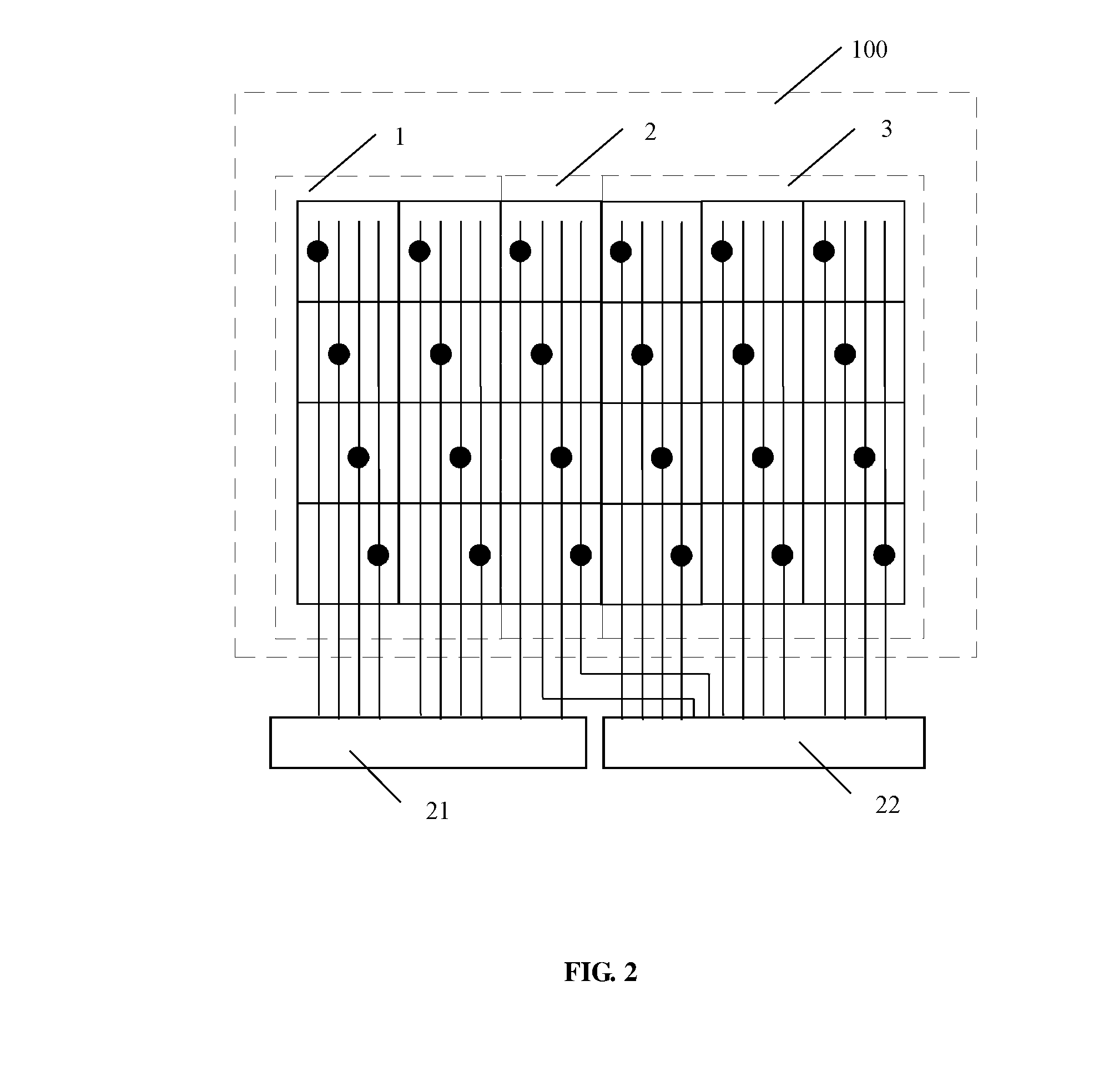
[0028]Referring to FIG. 2 in combination with FIG. 1, an array substrate according to the present disclosure is illustrated, which is adapted to eliminate vision disparity at a transition area of different display regions.
[0029]The array substrate includes: a display region 100 and a non-display region 200. The non-display region 200 includes a first non-display region 201 located on a left side of the display region 100, a second non-display region 202 located on a right side of the display region 100, and a third non-display region 203 located below the display region 100. The display region 100 at least includes a first display region 1, a second display region 2, and a third display region 3 arranged in sequence. The non-display region 200 at least includes a first control module 21 and a second control module 22.
[0030]The display region 100 is configured with a plurality of electrode blocks, the electrode blocks located in the first display region 1 are all connected with the f...
second embodiment
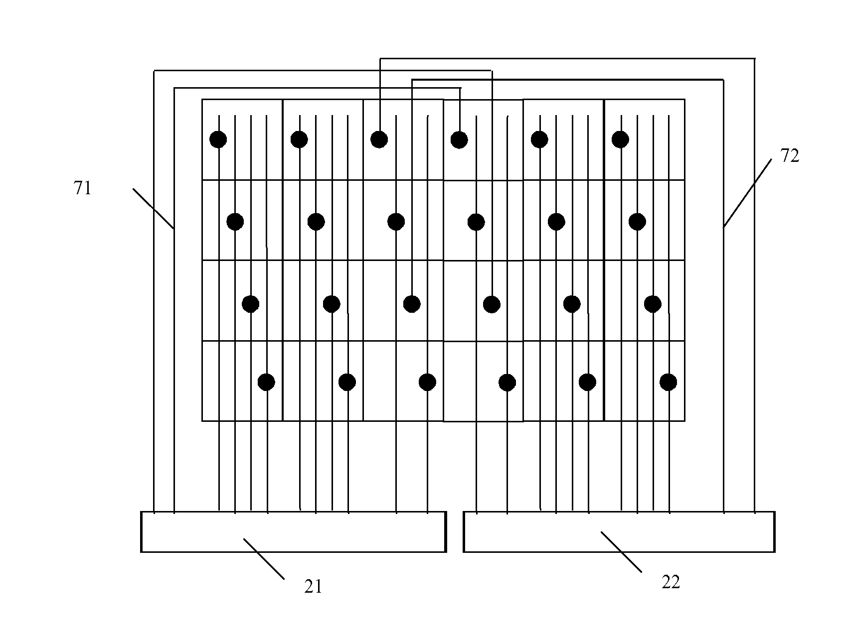
[0033]As shown in FIG. 2, the second display region only includes one column of electrode blocks. Hereafter, we will illustrate the second region under condition of including two columns of electrode blocks, as shown in FIG. 3. Referring to FIG. 3, an array substrate according to the present disclosure is illustrated. The second region includes two columns of electrode blocks, that is, a first column of electrode blocks and a second column of electrode blocks. In the first column of electrode blocks, some of the electrode blocks are connected with the first control module 21, and some of the electrode blocks are connected with the second control module 22 Similarly, in the second column of electrode blocks, some of the electrode blocks are connected with the first control module 21, and some of the electrode blocks are connected with the second control module 22.
third embodiment
[0034]The connection configuration (i.e. the connections to the first and second control modules) can also be designed in the way as shown in FIG. 4. Referring to FIG. 4, an array substrate according to the present disclosure is illustrated. Specifically, the second region includes a first column of electrode blocks which is located on a left side of the second region and a second column located of electrode blocks which is located on a right side of the second region. In the first column of electrode blocks, some of the electrode blocks are connected with the first control module 21, and some of the electrode blocks are connected with the second control module 22. In the second column of electrode blocks, all the electrode blocks are connected with the second control module 22.
PUM
 Abstract
Description
Claims
Application Information