Solid-state imaging device, imaging system, and signal processing method
a solid-state imaging and imaging system technology, applied in the direction of solid-state device signal generators, picture signal generators, television systems, etc., can solve the problem of reducing the dynamic range of output signals, and achieve the effect of suppressing the degradation of image quality
- Summary
- Abstract
- Description
- Claims
- Application Information
AI Technical Summary
Benefits of technology
Problems solved by technology
Method used
Image

Examples
first embodiment
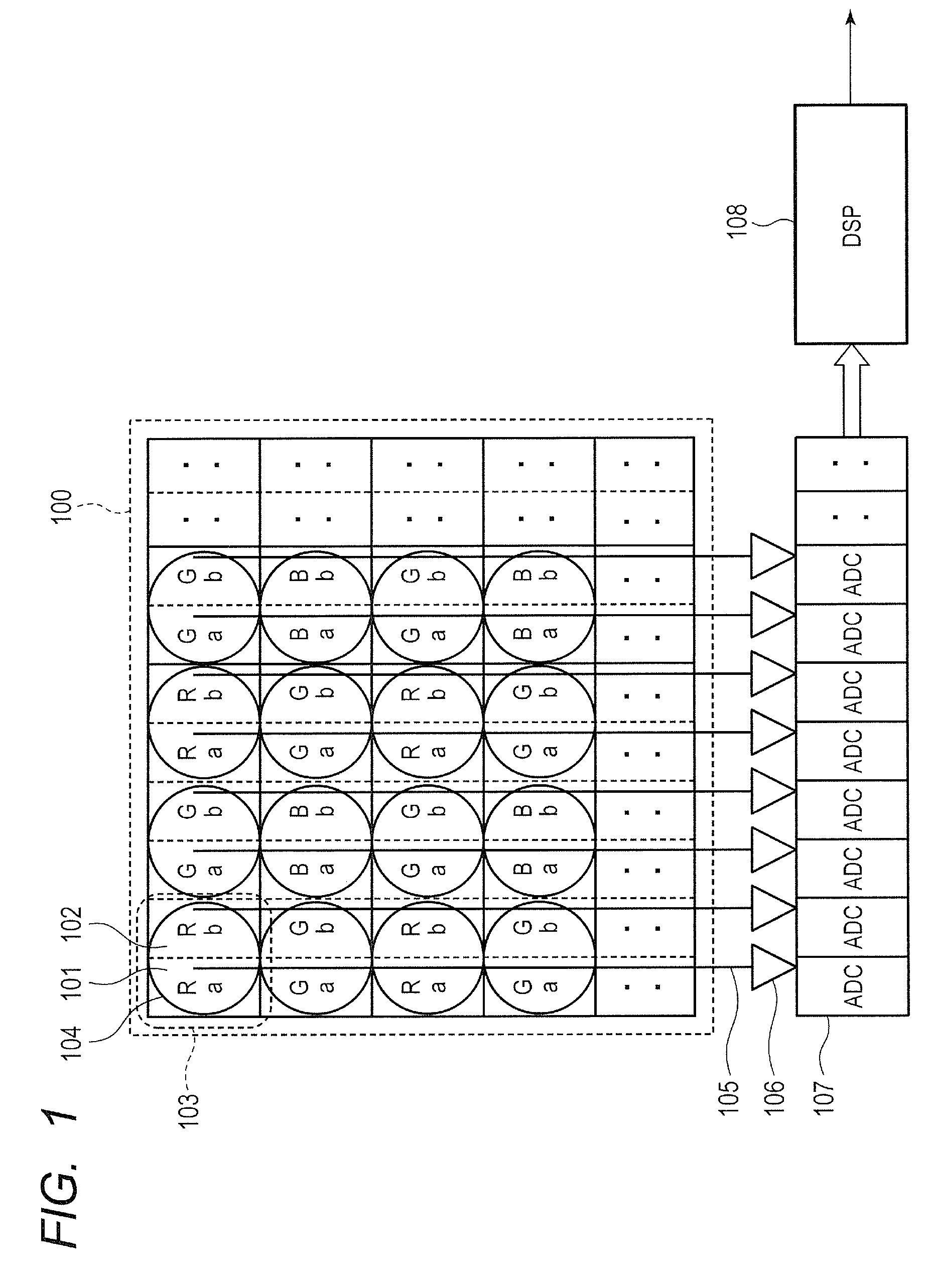
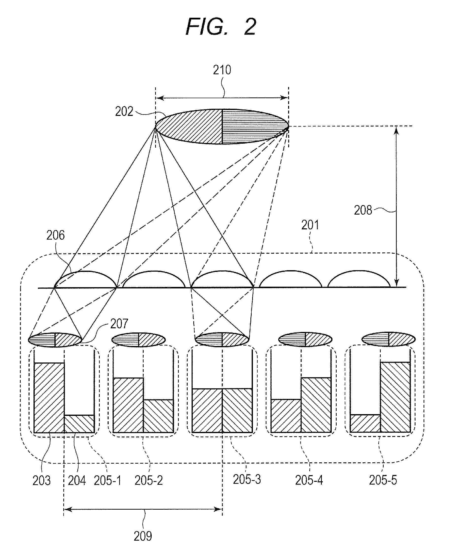
[0022]A solid-state imaging device and a signal processing method according to a first embodiment of the present invention will be described with reference to FIGS. 1 to 5.
[0023]FIG. 1 is a schematic view illustrating a configuration example of the solid-state imaging device according to the present embodiment. FIG. 2 is a schematic cross-sectional view illustrating an example of an imaging unit including the solid-state imaging device according to the present embodiment. FIG. 3 is a graph illustrating an example of input-output characteristics before a signal processing according to the present embodiment. FIG. 4 is a flowchart illustrating a signal processing method in the solid-state imaging device according to the present embodiment. FIG. 5 is a graph illustrating an example of input-output characteristics after the signal processing according to the present embodiment.
[0024]First, the structure of the solid-state imaging device according to the present embodiment is described w...
second embodiment
[0053]A solid-state imaging device and a signal processing method according to a second embodiment of the present invention will be described with reference to FIGS. 6 to 9. Components which are the same as the components in the solid-state imaging device and the signal processing method according to the first embodiment illustrated in FIGS. 1 to 5 are denoted by the same reference numerals and descriptions thereof are omitted or simplified.
[0054]FIG. 6 is a graph illustrating another example of input-output characteristics before the signal processing in the first embodiment. FIG. 7 is a graph illustrating an example of input-output characteristics after the signal processing in the first embodiment on the input-output characteristics of FIG. 6. FIG. 8 is a flowchart illustrating the signal processing method in the solid-state imaging device according to the present embodiment. FIG. 9 is a graph illustrating an example of input-output characteristics obtained by the signal processi...
third embodiment
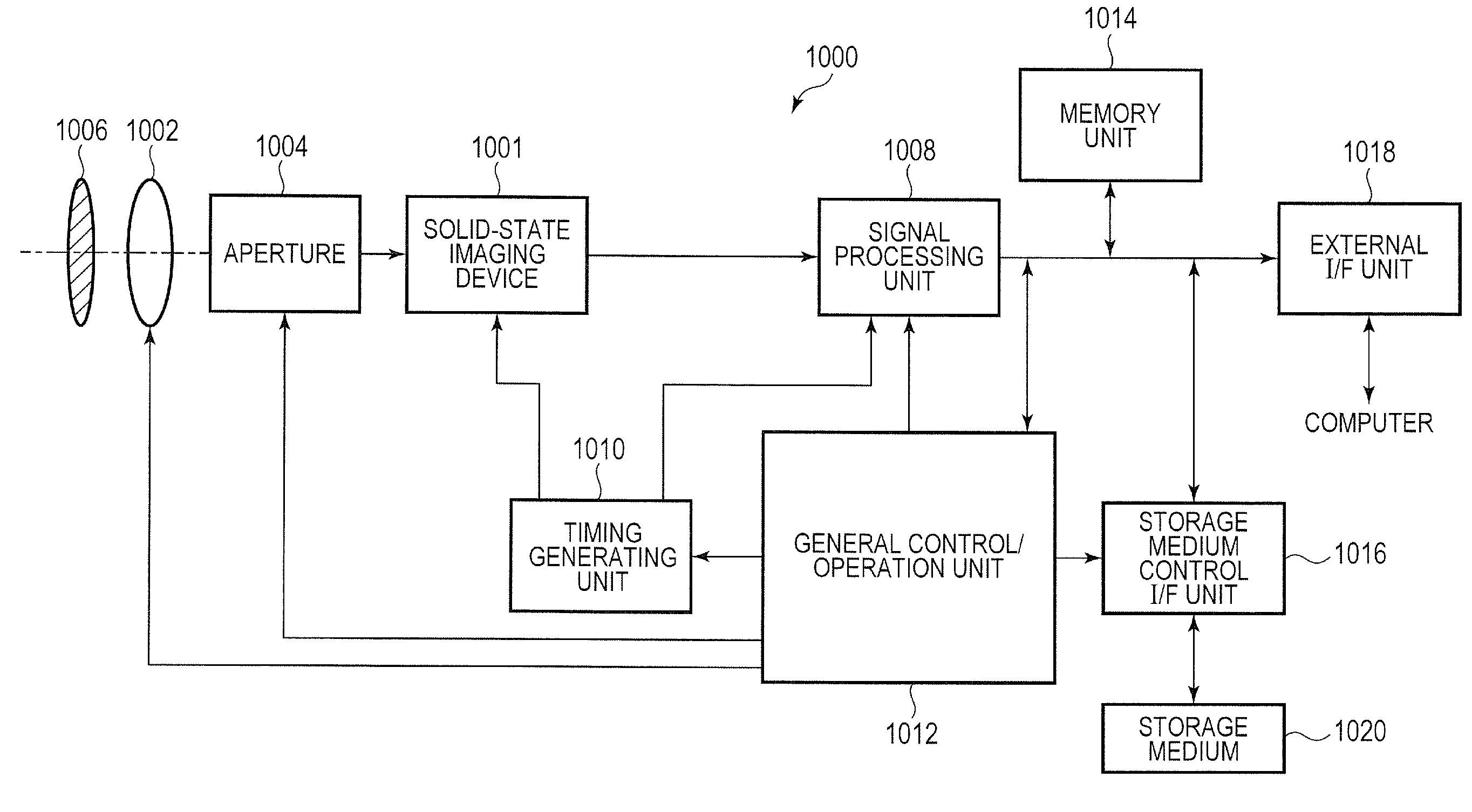
[0074]An imaging system according to a third embodiment of the present invention will be described with reference to FIG. 10. FIG. 10 is a block diagram illustrating a schematic configuration of the imaging system according to the present embodiment. Components which are the same as the components in the solid-state imaging devices in the first and second embodiments illustrated in FIGS. 1 to 9 are denoted by the same reference numerals and descriptions thereof are omitted or simplified.
[0075]An imaging system 1000 according to the present embodiment is not limited to a particular system, and can be applied to, for example, a digital still camera, a digital camcorder, a camera head, a photocopier, a fax machine, a mobile phone, a vehicle-mounted camera, an observation satellite, and the like.
[0076]As illustrated in FIG. 10, the imaging system 1000 includes a solid-state imaging device 1001, a lens 1002, an aperture 1004, a barrier 1006, a signal processing unit 1008, a timing genera...
PUM
 Abstract
Description
Claims
Application Information
 - R&D
- Intellectual Property
- Life Sciences
- Materials
- Tech Scout
- Unparalleled Data Quality
- Higher Quality Content
- 60% Fewer Hallucinations
Browse by: Latest US Patents, China's latest patents, Technical Efficacy Thesaurus, Application Domain, Technology Topic, Popular Technical Reports.
© 2025 PatSnap. All rights reserved.Legal|Privacy policy|Modern Slavery Act Transparency Statement|Sitemap|About US| Contact US: help@patsnap.com