Solid state imaging device, method for driving the same, and camera

a technology of solid state imaging and drive mode, which is applied in the direction of radio frequency controlled devices, instruments, television systems, etc., can solve the problems of inability to obtain accurate images, image degradation, and large degraded image quality of images created in accordance with signals read from row memories, so as to improve picture quality, improve picture quality, and save time spent on reading operation

Active Publication Date: 2009-07-28
GK BRIDGE 1
View PDF9 Cites 7 Cited by
  • Summary
  • Abstract
  • Description
  • Claims
  • Application Information

AI Technical Summary

Benefits of technology

[0013]The solid state imaging device of this invention includes the plural first memories for storing the signals of the selected first pixels out of the plural first pixels and the plural second memories respectively connected to the first memories in parallel for storing the signals of the selected second pixels out of the plural second pixels. Therefore, the operation for reading signals from pixels and storing them in memories and the operation for outputting the signals stored in the memories can be performed in parallel. Accordingly, there is no need to complete the operation for reading the signals from the pixels and storing them in the memories within a horizontal blanking period included in a horizontal drive period besides a vertical blanking period, and hence, time for storing the signals in the memories can be sufficiently secured. As a result, the signals can be stably stored in the memories and can be stably read from the memories in the present solid state imaging device.
[0015]The solid state imaging device of the invention may further include a plurality of drive pulse lines for driving the plurality of first pixels and the plurality of second pixels, and at least one of the operation for reading the signals stored in the first memories to the horizontal signal line and the operation for outputting the signals from the output amplifier or at least one of the operation for reading the signals stored in the second memories to the horizontal signal line and the operation for outputting the signals from the output amplifier is preferably stopped while a drive pulse is being applied to at least one of the plurality of drive pulse lines. Thus, it is possible to suppress degradation in picture quality caused when noise derived from the drive pulse is superposed on a signal output from a memory.
[0016]Alternatively, at least one of the operation for reading the signals stored in the first memories to the horizontal signal line and the operation for outputting the signals from the output amplifier or at least one of the operation for reading the signals stored in the second memories to the horizontal signal line and the operation for outputting the signals from the output amplifier is preferably stopped at a rise and a fall of a drive pulse applied to at least one of the plurality of first pixels and the plurality of second pixels. Thus, noise derived from the drive pulse can be prevented from being superposed on a signal output from a memory and increase in time required for outputting signals from memories can be suppressed.
[0019]In the solid state imaging device of the invention, the operation for storing the signals of the selected first pixels out of the plurality of first pixels in the first memories and the operation for storing the signals of the selected second pixels out of the plurality of second pixels in the second memories are preferably performed over a horizontal blanking period and a horizontal active period that is included neither in a vertical blanking period nor in a horizontal blanking period. Thus, even when the horizontal blanking period is short, time spent on the operation for reading the signals from the pixels can be sufficiently secured, so as to largely improve the picture quality.
[0020]In the solid state imaging device of the invention, at least a part of the operation for reading the signals stored in the first memories to the horizontal signal and the operation for outputting the signals from the output amplifier is preferably performed in parallel with at least a part of the operation for storing the signals of the selected second pixels out of the plurality of second pixels in the second memories in one horizontal blanking period, and at least a part of the operation for reading the signals stored in the second memories to the horizontal signal and the operation for outputting the signals from the output amplifier is preferably performed in parallel with at least a part of the operation for storing the signals of the selected first pixels out of the plurality of first pixels in the first memories in another horizontal blanking period. Thus, even when the horizontal drive period is short, the time spent on the operation for reading the signals from the pixels can be sufficiently secured, so as to largely improve the picture quality.
[0024]In the method for driving a solid state imaging device of this invention, an operation for reading signals from pixels and storing them in memories and an operation for outputting signals stored in the memories can be performed in parallel. Accordingly, there is no need to complete the operation for reading the signals from the pixels and storing them in the memories within a horizontal blanking period included in a horizontal drive period besides a vertical blanking period, and hence, time for storing the signals in the memories can be sufficiently secured.

Problems solved by technology

In the conventional solid state imaging device, if signals are read from pixels and the read signals are stored in row memories in the horizontal active period included in the horizontal drive period besides the vertical blanking period, signals of pixels on an (n+1)th row are overwritten on signals of pixels on the nth row remaining in the row memories 123, and therefore, an accurate image cannot be obtained and the image is disadvantageously degraded.
Accordingly, signals stored in row memories exhibit unstable values, and hence, there arises a problem that the quality of an image created in accordance with the signals read from the row memories is largely degraded.

Method used


Image

  • Solid state imaging device, method for driving the same, and camera
  • Solid state imaging device, method for driving the same, and camera
  • Solid state imaging device, method for driving the same, and camera

Examples


embodiment 1

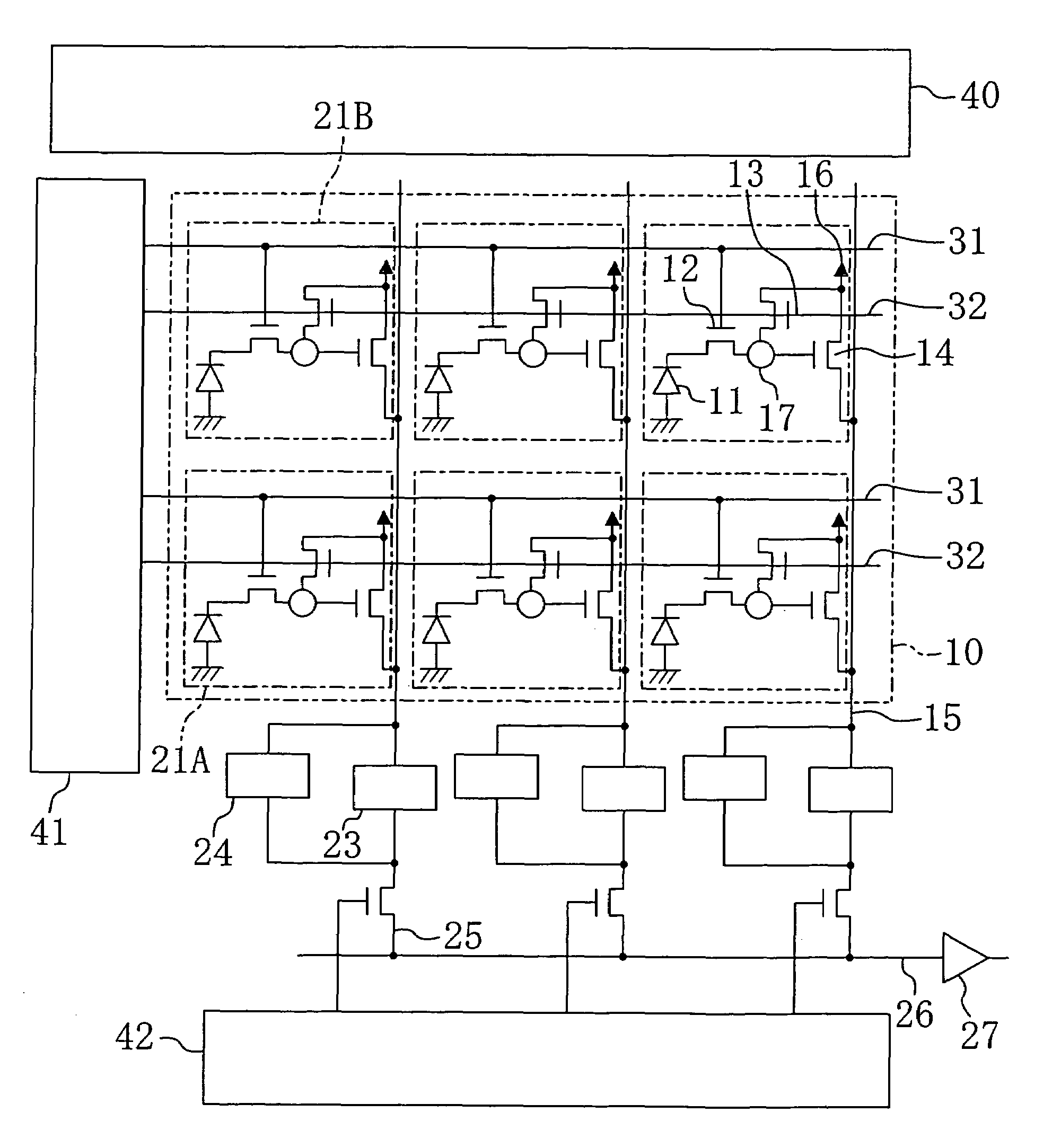
[0036]Embodiment 1 of the invention will now be described with reference to the accompanying drawings. FIG. 1 shows the circuit configuration of a solid state imaging device according to Embodiment 1 of the invention. As shown in FIG. 1, the solid state imaging device of this embodiment has an imaging area 10 where a plurality of amplifying unit pixels 21 are arranged in the form of a matrix. Although the imaging area 10 shown in FIG. 1 has a matrix of two rows by three columns, the numbers of rows and columns can be arbitrarily set.

[0037]Each pixel 21 includes a photoelectric conversion portion (PD portion) 11 of a photodiode formed on a semiconductor substrate and a floating diffusion (FD) portion 17 connected to the PD portion 11 through a read transistor 12 for storing charge of the PD portion 11. The FD portion 17 is connected to a VDD power supply 16 through a reset transistor 13 and to a vertical signal line 15 through a detection transistor 14.

[0038]The gate of the read tran...

modification 1

of Embodiment 1

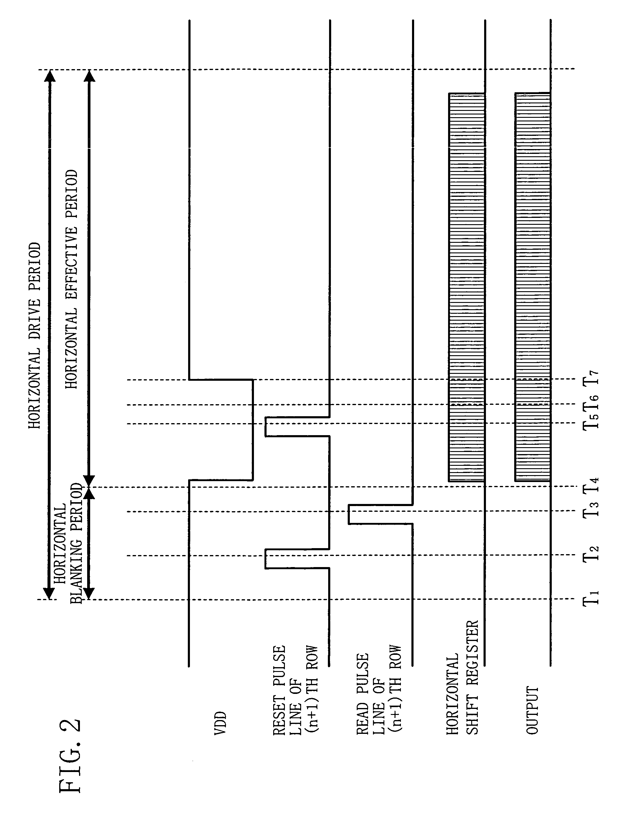
[0051]FIG. 3 is a timing chart in a horizontal drive period besides a vertical blanking period of a solid state imaging device according to Modification 1 of Embodiment 1. The solid state imaging device of this modification has the same circuit configuration as the solid state imaging device of Embodiment 1. In the solid state imaging device of this modification, while a reset pulse is being applied to the reset pulse line 32, the operation of the horizontal shift register 42 and the operation of the output amplifier 27 for outputting signals are stopped.

[0052]In the case where the operation for reading the signals from the respective pixels 21B of the (n+1)th row and storing them in the second memories 24 and the operation for outputting the signals of the respective pixels 21A of the nth row from the first memories 23 are performed in parallel, it is apprehended that when a reset pulse is applied from the reset pulse line 32 to the respective pixels 21B of the (n+1)...

modification 2

of Embodiment 1

[0057]FIG. 4 is a timing chart in a horizontal drive period besides a vertical blanking period of a solid state imaging device according to Modification 2 of Embodiment 1. The solid state imaging device of this modification has the same circuit configuration as the solid state imaging device of Embodiment 1. In the solid state imaging device of this modification, the operation of the horizontal shift register 42 and the operation of the output amplifier 27 for outputting signals are stopped at a rise and a fall of a drive pulse applied to a drive pulse line such as the reset pulse line 32.

[0058]Noise derived from a drive pulse is easily caused at a rise and a fall of the drive pulse. Therefore, when the operation for reading a signal from a memory is stopped at a rise and a fall of a drive pulse, a signal substantially free from noise derived from the drive pulse can be obtained and time for stopping the output operation can be short.

[0059]As a result, the operation f...


PUM


Abstract

A solid state imaging device includes an imaging area where a plurality of first pixels and a plurality of second pixels are respectively arranged in the form of a matrix, each of the first pixels and the second pixels having a photoelectric conversion portion and outputting a signal in accordance with brightness of incident light when selected; a plurality of first memories that respectively store signals of selected first pixels out of the plurality of first pixels; and a plurality of second memories that are respectively connected in parallel to the first memories and respectively store signals of selected second pixels out of the plurality of second pixels. The signals stored in the first memories and in the second memories are successively read to a horizontal signal line.

Description

CROSS-REFERENCE TO RELATED APPLICATIONS[0001]This application claims priority under 35 U.S.C. §119 on patent application Ser. No. 2005-333322 filed in Japan on Nov. 17, 2005, the entire contents of which are hereby incorporated by reference.BACKGROUND OF THE INVENTION[0002]The present invention relates to a solid state imaging device, a method for driving the same, and a camera, and more particularly, it relates to a solid state imaging device for use in a high-definition camera or the like, a method for driving the same, and a camera using the same.[0003]FIG. 7 shows an exemplified conventional solid state imaging device including MOS transistors. As shown in FIG. 7, the solid state imaging device has an imaging area 120 where a plurality of amplifying unit pixels are two-dimensionally arranged. Each amplifying unit pixel includes a photodiode (PD) portion 111; a floating diffusion portion (FD) 117 connected to the PD portion 111 through a read transistor 112 for storing charge rea...

Claims


Application Information

Patent Timeline
Patent Type & Authority Patents(United States)
IPC IPC(8): H04N3/14H04N5/335H01L27/146H04N5/369H04N5/374H04N5/3745H04N5/376H04N5/378
CPCH04N5/3742H04N5/3741H04N25/766H04N25/767
Inventor YAMAGUCHI, TAKUMIMURATA, TAKAHIKOKASUGA, SHIGETAKAYAMADA, TAKAYOSHIMATSUNAGA, YOSHIYUKIMIYAGAWA, RYOHEI
Owner GK BRIDGE 1
Why Eureka
Try Eureka