Solid-state imaging device, method of driving solid-state imaging device, imaging system, and movable object

a technology of solid-state imaging and imaging device, which is applied in the direction of color television, television system, radio control device, etc., can solve the problem of image quality decline, and achieve the effect of suppressing the decline in image quality

Active Publication Date: 2019-12-10
CANON KK
View PDF105 Cites 7 Cited by
  • Summary
  • Abstract
  • Description
  • Claims
  • Application Information

AI Technical Summary

Benefits of technology

[0005]An object of the present invention is to provide a solid-state imaging device and a method of driving the same that can suppress a decrease in image quality when configured to transfer charges from a photoelectric converter to a holding portion for multiple times during an exposure period.

Problems solved by technology

In the configuration of transferring charges from a photoelectric converter to a holding portion for multiple times during an exposure period, however, the image quality may decrease.

Method used


Image

  • Solid-state imaging device, method of driving solid-state imaging device, imaging system, and movable object
  • Solid-state imaging device, method of driving solid-state imaging device, imaging system, and movable object
  • Solid-state imaging device, method of driving solid-state imaging device, imaging system, and movable object

Examples


first embodiment

[0026]A solid-state imaging device and a method of driving the same according to a first embodiment of the present invention will be described with reference to FIG. 1 to FIG. 6.

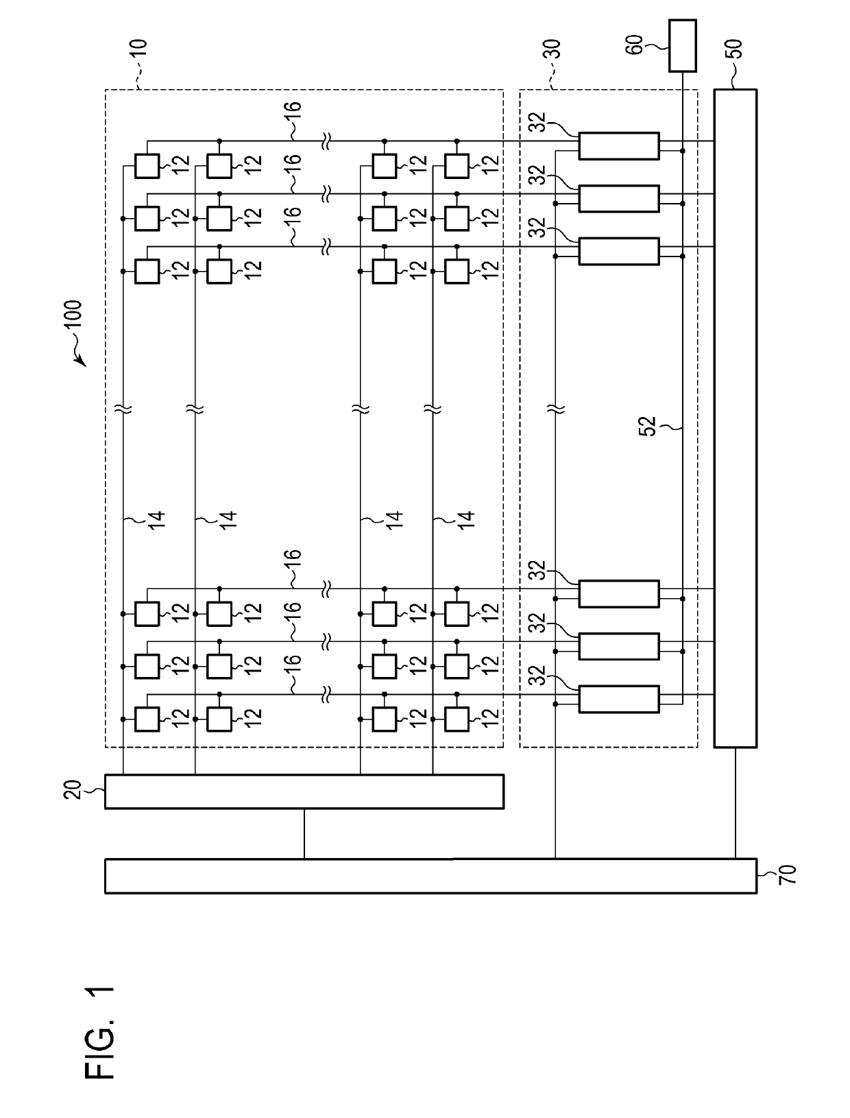
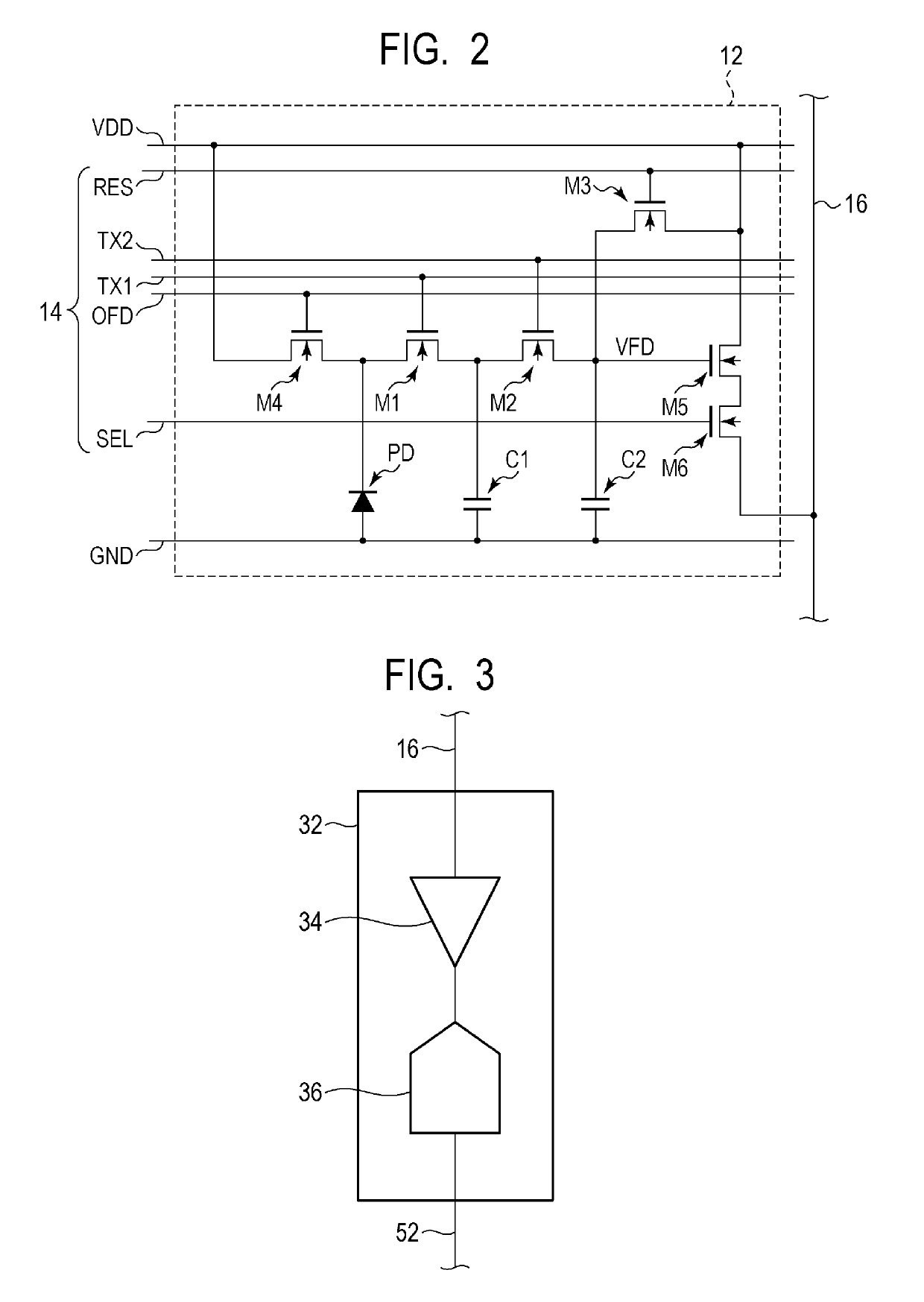
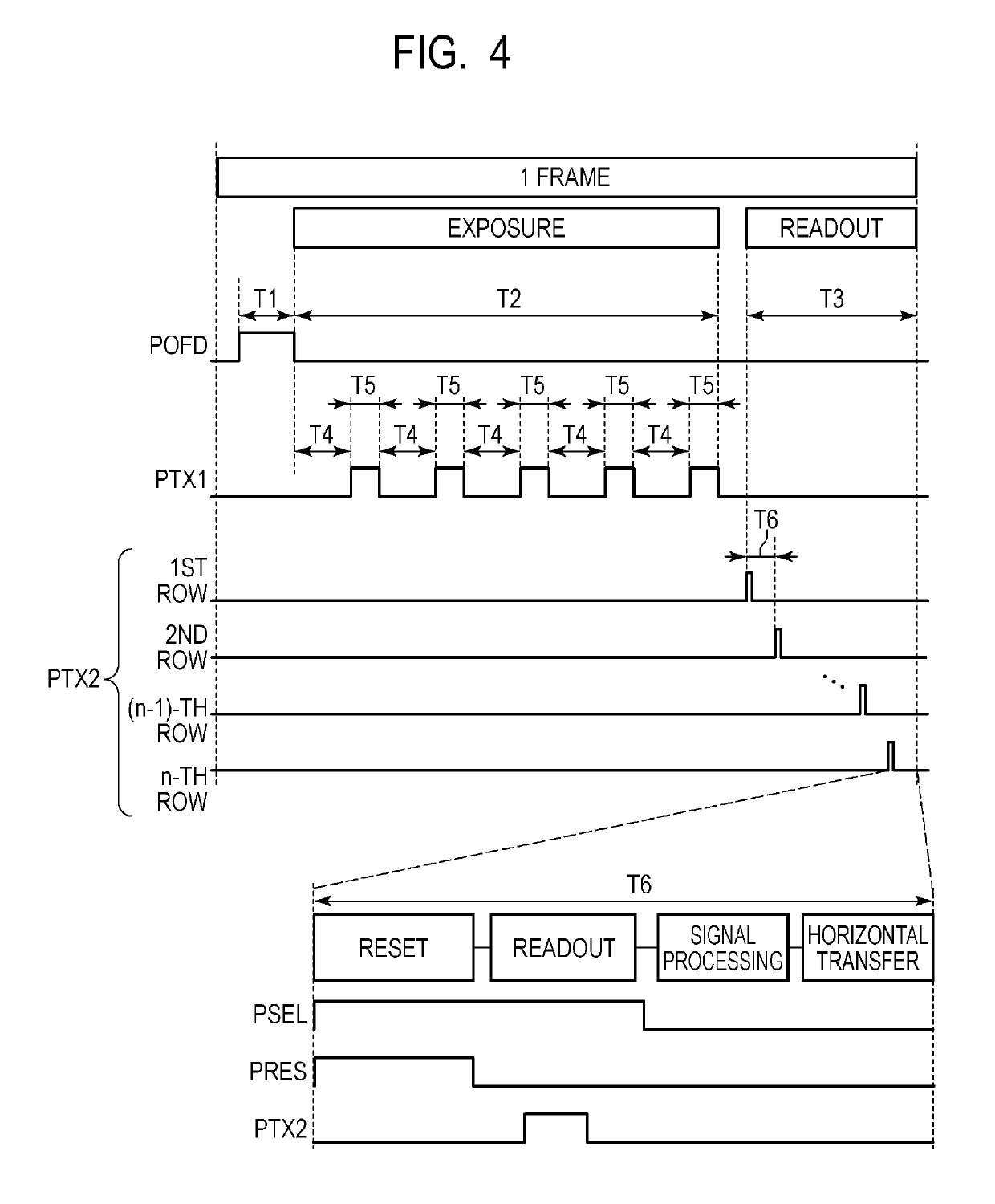
[0027]FIG. 1 is a block diagram illustrating a general configuration of a solid-state imaging device according to the present embodiment. FIG. 2 is a circuit diagram illustrating an example configuration of a pixel of the solid-state imaging device according to the present embodiment. FIG. 3 is a block diagram illustrating an example configuration of a column signal processing unit of the solid-state imaging device according to the present embodiment. FIG. 4 is a timing diagram illustrating a method of driving the solid-state imaging device according to the present embodiment. FIG. 5 and FIG. 6 are diagrams illustrating example settings of the number of transfers and the gain in the method of driving the solid-state imaging device according to the present embodiment.

[0028]First, the structure of the solid-st...

second embodiment

[0079]A solid-state imaging device and a method of driving the same according to a second embodiment of the present invention will be described with reference to FIG. 7 to FIG. 10. Components similar to those of the solid-state imaging device of the first embodiment are labeled with the same reference numerals, and the description thereof will be omitted or simplified.

[0080]FIG. 7 is a timing diagram illustrating an example drive operation of a solid-state imaging device when the number of transfers is two. FIG. 8 is a diagram illustrating an example setting of the number of transfers and a gain in the example drive operation of FIG. 7. FIG. 9 is a timing diagram illustrating the method of driving the solid-state imaging device according to the present embodiment. FIG. 10 is a diagram illustrating an example setting of the number of transfers and a gain in the method of driving the solid-state imaging device according to the present embodiment.

[0081]In the present embodiment, anothe...

third embodiment

[0093]A solid-state imaging device and a method of driving the same according to a third embodiment of the present invention will be described with reference to FIG. 11. Components similar to those of the solid-state imaging device of the first and second embodiments are labeled with the same reference numerals, and the description thereof will be omitted or simplified.

[0094]FIG. 11 is a timing diagram illustrating the method of driving the solid-state imaging device according to the present embodiment. In the present embodiment, another method of driving the solid-state imaging device according to the first embodiment illustrated in FIG. 1 to FIG. 3 will be described. In the present embodiment, a method of controlling accumulation time when distributing the accumulation time by using the transfer transistor M4 will be described.

[0095]As an example application to the first embodiment, it is assumed here that the ratio of the saturation charge amount QP of the photoelectric converter...


PUM


Abstract

A solid-state imaging device includes pixels each of which includes a photoelectric converter configured to generate charges by photoelectric conversion, a holding unit configured to hold charges generated by the photoelectric converter, and a transfer unit configured to transfer charges from the photoelectric converter to the holding unit, and outputs a signal based on charges in the holding unit, a transfer control unit configured to control the transfer unit to transfer charges generated by the photoelectric converter during one exposure period to the holding unit by a variable number, which is one or greater, of transfer operations, an amplifier unit configured to amplify the signal, and a control unit configured to control a gain of the amplifier unit to be a first gain when the number of transfer operations is first number and to be a second gain when the number of transfer operations is a second number.

Description

BACKGROUND OF THE INVENTIONField of the Invention[0001]The present invention relates to a solid-state imaging device and a method of driving solid-state imaging device.Description of the Related Art[0002]In recent years, a CMOS image sensor having a global electronic shutter function has been proposed. The global electronic shutter refers to electric control of a capturing operation such that exposure periods are the same among a plurality of pixels. A use of global electronic shutter has an advantage that an object image is less likely to be distorted even when capturing an object moving fast.[0003]Japanese Patent Application Laid-Open No. 2015-177349 discloses that a solid-state imaging device having a global electronic shutter function is configured to transfer charges from a photoelectric converter to a holding portion for multiple times during an exposure period, which results in an increase of the saturation charge amount of a pixel while suppressing an increase in pixel size....

Claims


Application Information

Patent Timeline
Patent Type & Authority Patents(United States)
IPC IPC(8): H01L27/146H04N5/353H04N5/235H04N5/3745H04N5/374H04N5/355
CPCH04N5/3532H04N5/2353H01L27/14609H04N25/50H04N25/60H04N25/70H04N25/57H04N25/59H04N25/767H04N25/771H04N23/73H04N25/531
Inventor KOBAYASHI, DAISUKEKOIZUMI, TORUSAITO, KAZUHIRO
Owner CANON KK
Why Eureka
Try Eureka