Liquid crystal display panel and device

a technology of liquid crystal display panel and display panel, which is applied in non-linear optics, instruments, optics, etc., can solve the problems of easy color shift problem, increased manufacturing cost, and affected display effect, so as to reduce manufacturing cost and increase the aperture ratio of pixel units. , the effect of reducing the manufacturing cos

Active Publication Date: 2016-10-27
TCL CHINA STAR OPTOELECTRONICS TECH CO LTD
View PDF6 Cites 0 Cited by
  • Summary
  • Abstract
  • Description
  • Claims
  • Application Information

AI Technical Summary

Benefits of technology

[0026]In the liquid crystal display panel and device of the present invention, the display domains patterns are formed by patterning the electrodes, thereby solving the technical problem that the display effect is poor when the double-sided display is implemented. Furthermore, each of the pixel units is divided into two subpixels which have the same area, such that the problem of color shift is solved when the subpixels are asymmetrical, the aperture ratio of the pixel units is increased, and the manufacturing cost is decreased.

Problems solved by technology

However, when the display domains which are formed as mentioned above display in a double-sided manner, viewing angles are different and thus display effect is affected.
Since each of the pixel units is divided asymmetrically, that is, the area of the first subpixel is larger than the area of the second subpixel, the problem of color shift easily occurs.
Furthermore, the charger-sharing thin film transistor and the sharing capacitor are required to be manufactured, and the manufacturing cost is increased.

Method used


Image

  • Liquid crystal display panel and device
  • Liquid crystal display panel and device
  • Liquid crystal display panel and device

Examples


Embodiment Construction

[0033]The following embodiments are referring to the accompanying drawings for exemplifying specific implementable embodiments of the present invention. Furthermore, directional terms described by the present invention, such as upper, lower, front, back, left, right, inner, outer, side and etc., are only directions by referring to the accompanying drawings, and thus the used directional terms are used to describe and understand the present invention, but the present invention is not limited thereto. In the drawings, structure-like elements are labeled with like reference numerals.

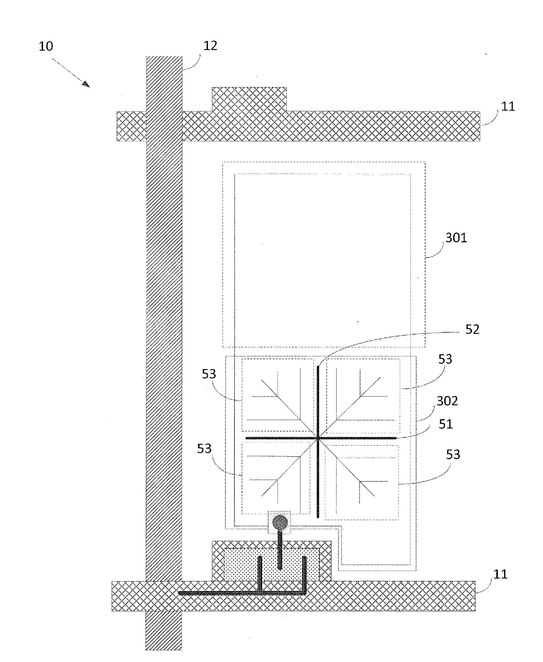
[0034]Please refer to FIG. 4. FIG. 4 is a structural diagram of an array substrate of a liquid crystal display panel in accordance with the present invention.

[0035]In conjunction with FIG. 6, the liquid crystal display panel comprises an array substrate 10, a color filter substrate 20, a liquid crystal layer 30, a pixel electrode 31, and a common electrode 32. The liquid crystal layer 30 is positioned betwe...


PUM

PropertyMeasurementUnit
areaaaaaaaaaaa
brightnessaaaaaaaaaa
viewing angleaaaaaaaaaa

Abstract

The present invention provides a liquid crystal display panel and device. The liquid crystal display panel includes a first subpixel and a second subpixel each having a plurality of display domains. The first subpixel includes a first pixel electrode and a first common electrode. The second subpixel includes a second pixel electrode and a second common electrode. The display domains of the first subpixel and the display domains of the second subpixel are respectively formed by patterning the first common electrode and the second pixel electrode.

Description

BACKGROUND OF THE INVENTION[0001]1. Field of the Invention[0002]The present invention generally relates to the technical field of a liquid crystal display, and more particularly to a liquid crystal display panel and device.[0003]2. Description of Prior Art[0004]A liquid crystal display device is widely utilized in human's life and work. A viewing angle, a brightness level, and a color directly affect display effect of the liquid crystal display device.[0005]In order to increase the viewing angle of a liquid crystal display panel, a pixel structure design with eight display domains is usually utilized. Each of pixel units is divided into two subpixels (one is large, and the other is small). A first subpixel comprises four display domains, and a second subpixel comprises four display domains. The display domains are formed by patterning pixel electrodes of the two subpixels.[0006]In conjunction with FIG. 3, a conventional liquid crystal display panel comprises an array substrate 10, a...

Claims


Application Information

Patent Timeline
Patent Type & Authority Applications(United States)
IPC IPC(8): G02F1/1343G02F1/1368G02F1/1362G02F1/1335
CPCG02F1/13439G02F1/133514G02F1/1368G02F1/136286G02F2201/123G02F2001/133342G02F2001/134345G02F2001/134318G02F2201/121G02F1/134309G02F1/134327G02F1/134318G02F1/133342G02F1/134345G02F1/1333
Inventor XU, XIANGYANG
Owner TCL CHINA STAR OPTOELECTRONICS TECH CO LTD
Why Eureka
Try Eureka