Display device, electronic device, and method for manufacturing display device

Pending Publication Date: 2022-06-02
SONY SEMICON SOLUTIONS CORP
View PDF0 Cites 0 Cited by
  • Summary
  • Abstract
  • Description
  • Claims
  • Application Information

AI Technical Summary

Benefits of technology

The present technology addresses the problem of uneven brightness in a display device caused by the directions of the chief rays being set perpendicular to the display surface, resulting in difficulty for the light to reach the viewer's eyes. The solution is a display device with multiple sub-pixels arranged on a predetermined surface, each containing a light-emitting portion and a reflector that reflects the emitted light in a direction towards the central axis of the display surface. This ensures that light is delivered to the viewer on the central axis, resulting in improved image quality.

Problems solved by technology

This can make it harder for the chief rays from the edges of the display device to reach the eyes of the viewer.
Consequently, there is a problem that unevenness in brightness occurs in an image viewed by the viewer, reducing the image quality.

Method used


Image

  • Display device, electronic device, and method for manufacturing display device
  • Display device, electronic device, and method for manufacturing display device
  • Display device, electronic device, and method for manufacturing display device

Examples


first embodiment

1. First Embodiment

Configuration Example of Electronic Device

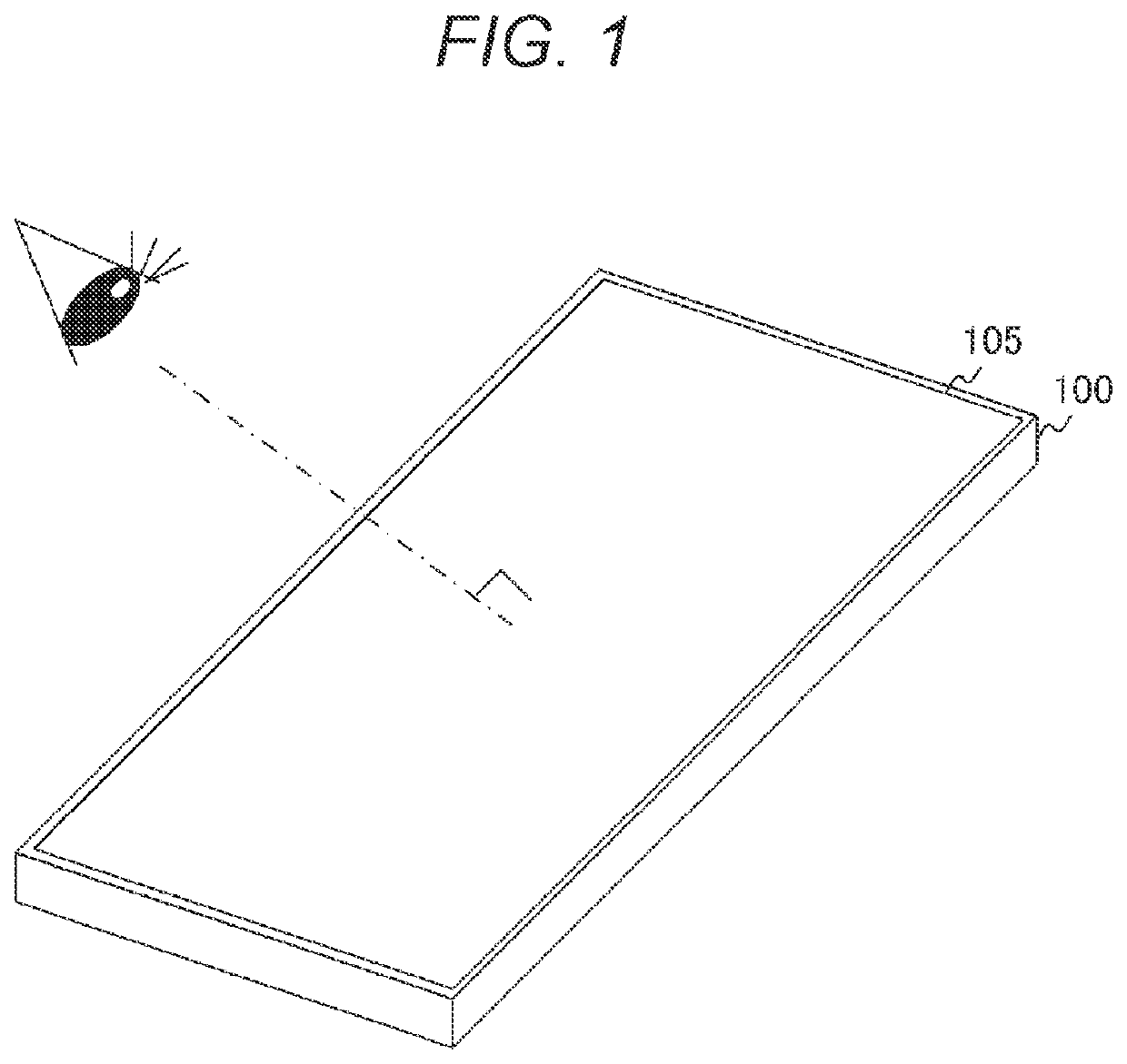
[0037]FIG. 1 is an example of an external view of an electronic device 100 according to a first embodiment of the present technology. The electronic device 100 is a device that can display various pieces of information such as images, and has a display surface 105 for displaying those pieces of information. As the electronic device 100, a mobile device such as a smartphone, a virtual reality (VR) terminal, or the like is assumed.

[0038]An axis that passes through the center of the display surface 105 and is perpendicular to the display surface 105 is hereinafter referred to as a “central axis”. A dot-dash line in the figure indicates the central axis. It is assumed that the line-of-sight direction when the viewer views an image displayed on the display surface 105 is mainly a direction along the central axis of the display surface 105.

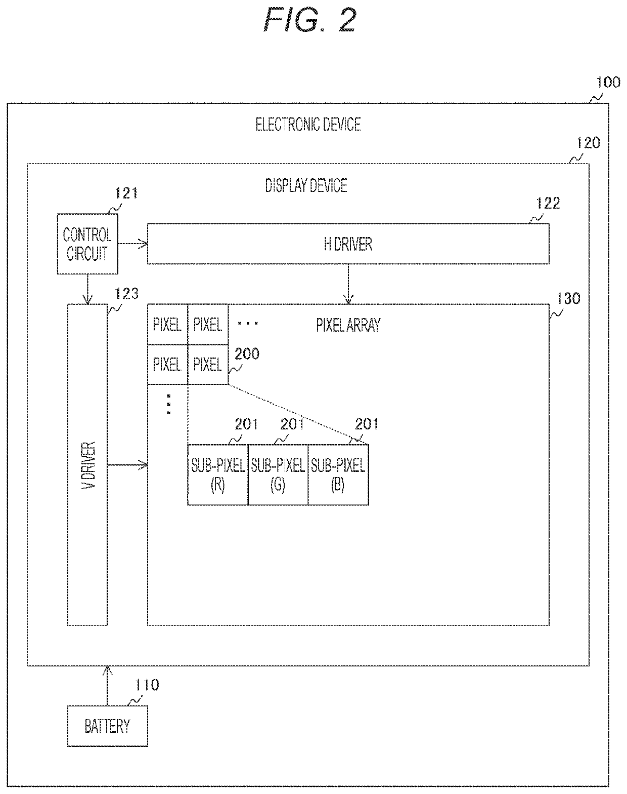
[0039]FIG. 2 is a block diagram illustrating a configuration example of the electronic dev...

second embodiment

2. Second Embodiment

[0091]In the first embodiment described above, the respective organic light-emitting layers 250 of the plurality of sub-pixels 201 self-emit light of R, G, and B. However, this configuration requires varying organic molecules in the organic light-emitting layers 250 for different colors, and can complicate the manufacturing process of the organic light-emitting layers 250. The display device 120 of the second embodiment is different from that of the first embodiment in that color filters are further provided at the sub-pixels 201.

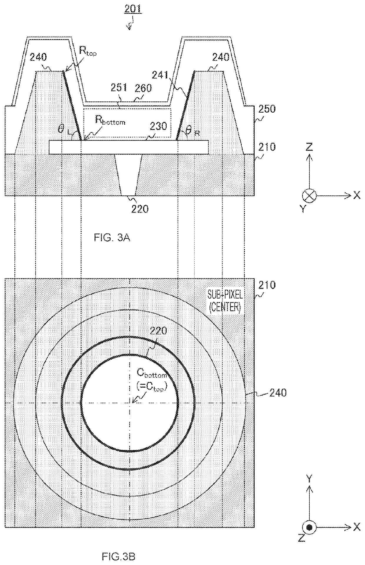
[0092]FIG. 15 is an example of a cross-sectional view and a top view of the central sub-pixel 201 according to the second embodiment of the present technology. In the figure, a is the example of the cross-sectional view of the sub-pixel 201, and b in the figure is the example of the top view thereof.

[0093]As illustrated in a of the figure, the sub-pixel 201 of the second embodiment is different from that of the first embodiment in that a...


PUM


Abstract

A display device provided with OLEDs improves the quality of an image. The display device includes a pixel array. A plurality of sub-pixels is arranged on the display surface of the pixel array. Furthermore, in the pixel array included in the display device, each of the plurality of sub-pixels is provided with a light-emitting portion and a reflector. At each of the plurality of sub-pixels arranged in the pixel array included in the display device, the reflector reflects light emitted from the light-emitting portion in a direction toward the central axis of the display surface.

Description

TECHNICAL FIELD[0001]The present technology relates to a display device. More specifically, the present technology relates to a display device using light-emitting elements, an electronic device, and a method for manufacturing the display device.BACKGROUND ART[0002]Organic light-emitting diodes (OLEDs) have conventionally been used in various display devices, with their characteristics such as allowing low power consumption and film thinning and high response speed taken into consideration. For example, a display device in which color filters of red (R), green (G), and blue (B) or the like and OLEDs are disposed at each pixel has been proposed (see, for example, Patent Document 1).CITATION LISTPatent Document[0003]Patent Document 1: Japanese Patent Application Laid-Open No. 2017-146372SUMMARY OF THE INVENTIONProblems To Be Solved By The Invention[0004]In the above conventional technique, the optical distances of the chief rays from the OLEDs are adjusted differently for each color o...

Claims


Application Information

Patent Timeline
IPC IPC(8): H01L51/52H01L27/32H01L51/56
CPCH01L51/5271H01L27/3246H01L2227/323H01L27/3283H01L27/322H01L51/56G09F9/00G09F9/30G09F9/302H05B33/12H05B33/02H10K59/38H10K59/122H10K2102/3023H10K71/00H10K59/878H10K50/856H10K59/173H10K59/1201
Inventor HIRAGA, KENTA
Owner SONY SEMICON SOLUTIONS CORP
Why Eureka
Try Eureka