In-cell touch panel

a technology of in-cell touch panel and capacitive touch panel, which is applied in the field of touch panel, can solve the problems that the in-cell capacitive touch panel cannot meet the thinnest thickness requirement of novel portable electronic products such as mobile phones, tablet pcs, notebooks, etc., and achieve the effects of enhancing the signal-noise ratio (snr), reducing the rc loading of the common electrode, and reducing the entire rc loading of the in-cell

Inactive Publication Date: 2016-11-17
RAYDIUM SEMICON
View PDF6 Cites 10 Cited by
  • Summary
  • Abstract
  • Description
  • Claims
  • Application Information

AI Technical Summary

Benefits of technology

[0032](3) The RC loading of the common electrode can be reduced.
[0033](4) When the in-cell touch panel is operated in touch mode, the common electrode is controlled simultaneously to reduce entire RC loading of the in-cell touch panel.
[0034](5) The touch mode and the display mode of the in-cell touch panel are driven in a time-sharing way to enhance the signal-noise ratio (SNR). The advantage and spirit of the invention may be understood by the following detailed descriptions together with the appended drawings.

Problems solved by technology

Compared to the conventional one glass solution (OGS), the on-cell capacitive touch panel can achieve thinner touch panel design; however, the on-cell capacitive touch panel cannot meet the thinnest thickness requirement of the novel portable electronic products such as mobile phones, tablet PCs, and notebooks.

Method used


Image

  • In-cell touch panel
  • In-cell touch panel
  • In-cell touch panel

Examples


first embodiment

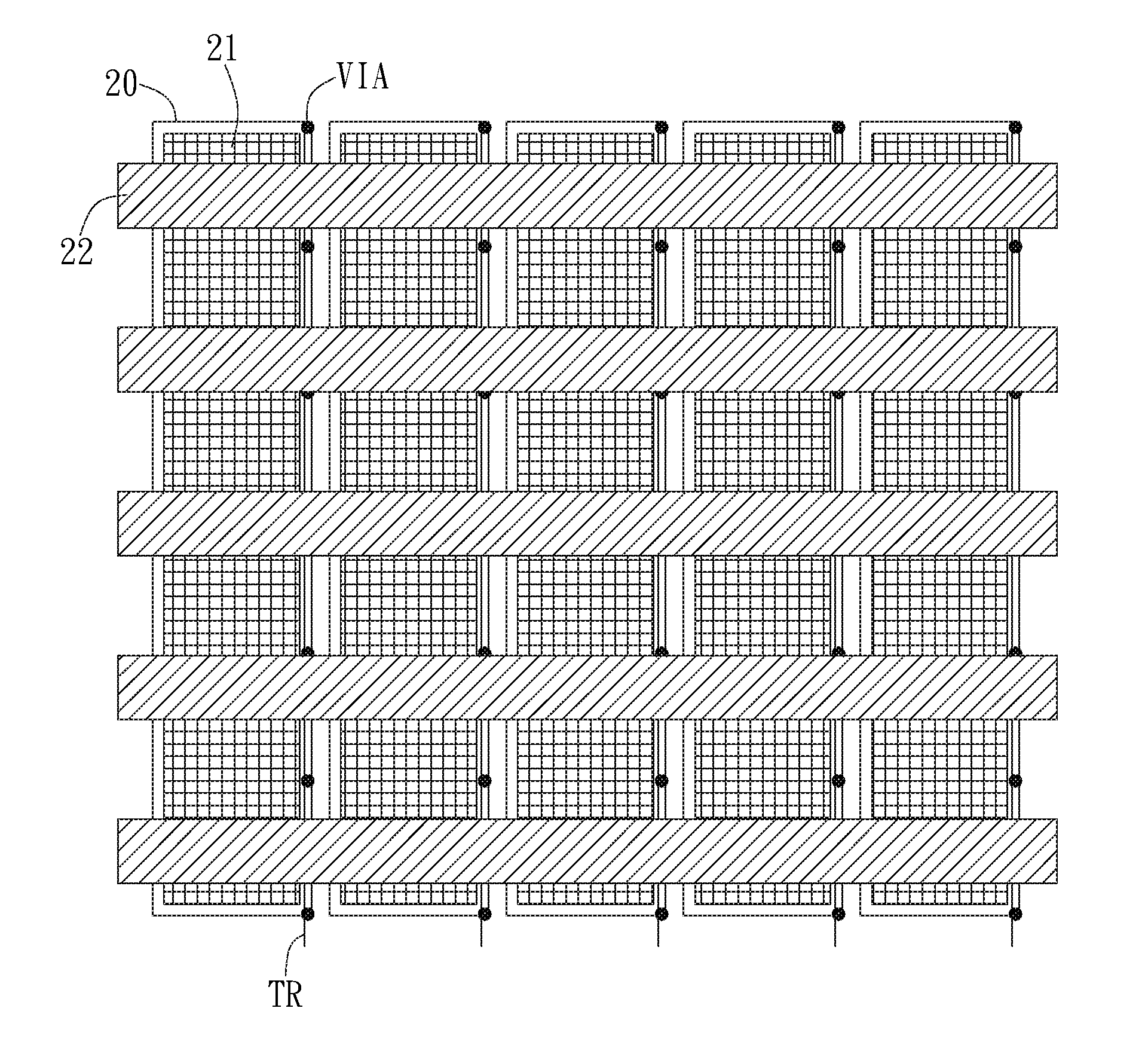
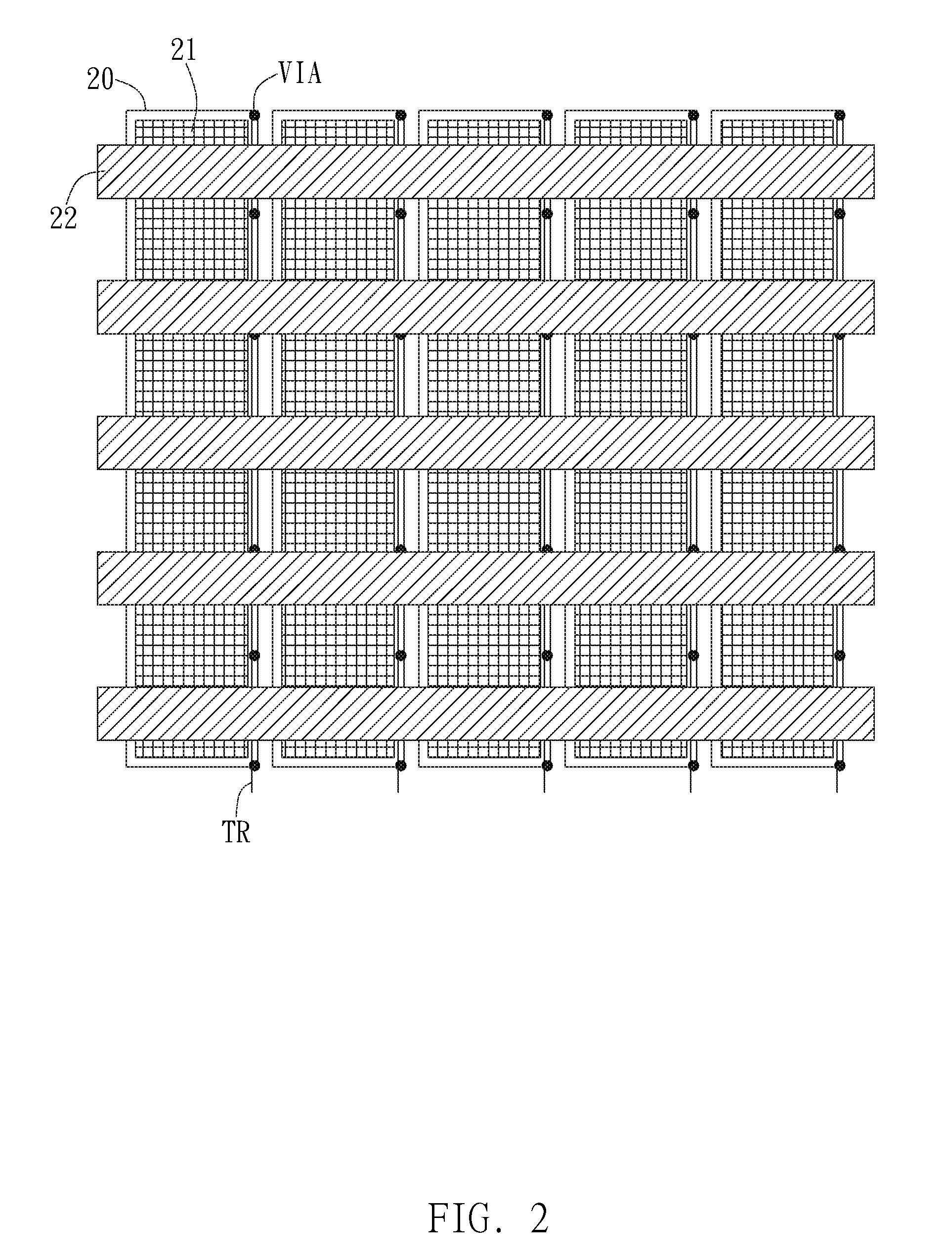
[0054]Then, please refer to FIG. 3A. FIG. 3A illustrates a cross-sectional schematic diagram of the laminated structure of the in-cell mutual-capacitive touch panel in the invention. As shown in FIG. 3A, the laminated structure 3 of the in-cell mutual-capacitive touch panel includes a substrate 30, a thin-film transistor (TFT) layer 31, a liquid crystal layer 32, a color filter layer 33, a glass layer 34, and a second conductive layer 35. The TFT layer 31 is disposed on the substrate 30. A first conductive layer 310 and a common electrode 312 are disposed in the TFT layer 31 and the first conductive layer 310 is formed after the common electrode 312 is formed. The first conductive layer 310 is arranged in mesh type. The liquid crystal layer 32 including a plurality of liquid crystal units LC is disposed above the TFT layer 31. The color filter layer 33 is disposed above the liquid crystal layer 32. The glass layer 34 is disposed above the color filter layer 33. The second conductive...

second embodiment

[0058]Then, please refer to FIG. 4A. FIG. 4A illustrates a cross-sectional schematic diagram of the laminated structure of the in-cell mutual-capacitive touch panel in the invention. As shown in FIG. 4A, the laminated structure 4 of the in-cell mutual-capacitive touch panel includes a substrate 40, a TFT layer 41, a liquid crystal layer 42, a color filter layer 43, a glass layer 44, and a second conductive layer 45. The TFT layer 41 is disposed on the substrate 40. A first conductive layer 410 and a common electrode 412 are disposed in the TFT layer 41 and the first conductive layer 410 is formed before the common electrode 412 is formed. The first conductive layer 410 is arranged in mesh type. The liquid crystal layer 42 including a plurality of liquid crystal units LC is disposed above the TFT layer 41. The color filter layer 43 is disposed above the liquid crystal layer 42. The glass layer 44 is disposed above the color filter layer 43. The second conductive layer 45 is disposed ...

third embodiment

[0062]Then, please refer to FIG. 5A. FIG. 5A illustrates a cross-sectional schematic diagram of the laminated structure of the in-cell mutual-capacitive touch panel in the invention. As shown in FIG. 5A, the laminated structure 5 of the in-cell mutual-capacitive touch panel includes a substrate 50, a TFT layer 51, a liquid crystal layer 52, a color filter layer 53, a glass layer 54, and a second conductive layer 55. The TFT layer 51 is disposed on the substrate 50. A first conductive layer 510 and a common electrode 512 are disposed in the TFT layer 51 and the first conductive layer 510 is formed after the common electrode 512 is formed. The first conductive layer 510 is arranged in mesh type. The liquid crystal layer 52 including a plurality of liquid crystal units LC is disposed above the TFT layer 51. The color filter layer 53 is disposed above the liquid crystal layer 52. The glass layer 54 is disposed above the color filter layer 53. The second conductive layer 55 is disposed a...


PUM

PropertyMeasurementUnit
conductiveaaaaaaaaaa
transparent conductiveaaaaaaaaaa
light resistanceaaaaaaaaaa

Abstract

An in-cell touch panel is disclosed. The in-cell touch panel includes a plurality of pixels. A laminated structure of each pixel includes a substrate, a TFT layer, a liquid crystal layer, a color filter layer, a glass layer and a second conductive layer. The TFT layer is disposed on the substrate. A first conductive layer and a common electrode are disposed in the TFT layer. The first conductive layer is arranged in mesh type. The liquid crystal layer is disposed above the TFT layer. The color filter layer is disposed above the liquid crystal layer. The glass layer is disposed above the color filter layer. The second conductive layer is disposed above the glass layer.

Description

BACKGROUND OF THE INVENTION[0001]1. Field of the Invention[0002]This invention relates to a touch panel, especially to an in-cell touch panel.[0003]2. Description of the Related Art[0004]Please refer to FIG. 1. FIG. 1 illustrates a laminated structure of a conventional on-cell capacitive touch panel. As shown in FIG. 1, the laminated structure 1 of the conventional on-cell capacitive touch panel includes a substrate 10, a thin-film transistor layer 11, a liquid crystal layer 12, a color filter layer 13, a glass layer 14, a touch sensing layer 15, a polarizer 16, an adhesive 17, and top cover lens 18.[0005]From FIG. 1, it can be found that the touch sensing layer 15 of the on-cell capacitive touch panel is disposed above the glass layer 14; that is to say, the touch sensing layer 15 is disposed out of the liquid crystal display module of the on-cell capacitive touch panel. Compared to the conventional one glass solution (OGS), the on-cell capacitive touch panel can achieve thinner to...

Claims


Application Information

Patent Timeline
Patent Type & Authority Applications(United States)
IPC IPC(8): G02F1/1333G02F1/1343G02F1/1368G02F1/1335G06F3/041G06F3/044
CPCG02F1/13338G06F3/0412G06F3/044G06F3/0416G02F2001/133302G02F1/133514G02F1/134309G06F2203/04112G02F1/1368G02F1/134363G02F2201/121G06F2203/04111G06F3/04184G06F3/0443G06F3/0445G06F3/0446G02F1/134318G02F1/133345G02F1/133512G02F1/133302
Inventor LIN, YI-YINGLEE, KUN-PEICHIANG, CHANG-CHING
Owner RAYDIUM SEMICON
Why Eureka
Try Eureka