In-cell touch panel and trace layout thereof

a technology of in-cell touch panel and trace layout, which is applied in the field of in-cell capacitive touch panel, can solve the problem that the thinnest thickness requirement of novel portable electronic products such as mobile phones, tablet pcs, notebooks, etc., and achieve the effect of reducing the loading of the common electrod

Inactive Publication Date: 2018-08-21
RAYDIUM SEMICON
View PDF15 Cites 2 Cited by
  • Summary
  • Abstract
  • Description
  • Claims
  • Application Information

AI Technical Summary

Benefits of technology

[0026]In an embodiment, the color filtering layer further includes a color filter and a black matrix resist and the black matrix resist has good light resistance, and the first conductive layer and the second conductive layer are disposed under the black matrix resist.
[0030]Compared to the prior arts, the in-cell mutual-capacitive touch panel and its trace layout of the invention have following advantages:
[0031](1) Designs of the touch electrodes and their traces in the in-cell touch panel of the invention are very simple, and the cost of the in-cell touch panel of the invention can be reduced.
[0032](2) Optical effects on the LCD touch panel can be reduced by the novel trace layout method of the invention, and the aperture ratio of the LCD touch panel can be enhanced.
[0033](3) The RC loading of the common electrode can be reduced by electrically connecting the non-touch electrode part of the first conductive layer and the second conductive layer with the common electrode.

Problems solved by technology

Compared to the conventional one glass solution (OGS), the on-cell capacitive touch panel can achieve thinner touch panel design; however, the on-cell capacitive touch panel cannot meet the thinnest thickness requirement of the novel portable electronic products such as mobile phones, tablet PCs, and notebooks.

Method used


Image

  • In-cell touch panel and trace layout thereof
  • In-cell touch panel and trace layout thereof
  • In-cell touch panel and trace layout thereof

Examples


Embodiment Construction

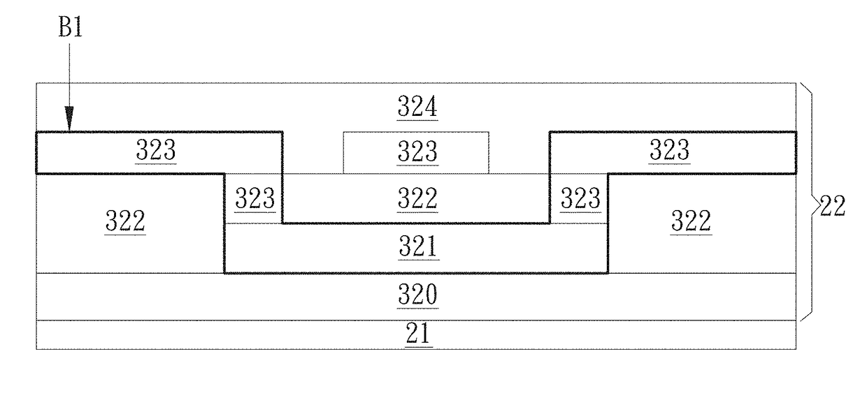
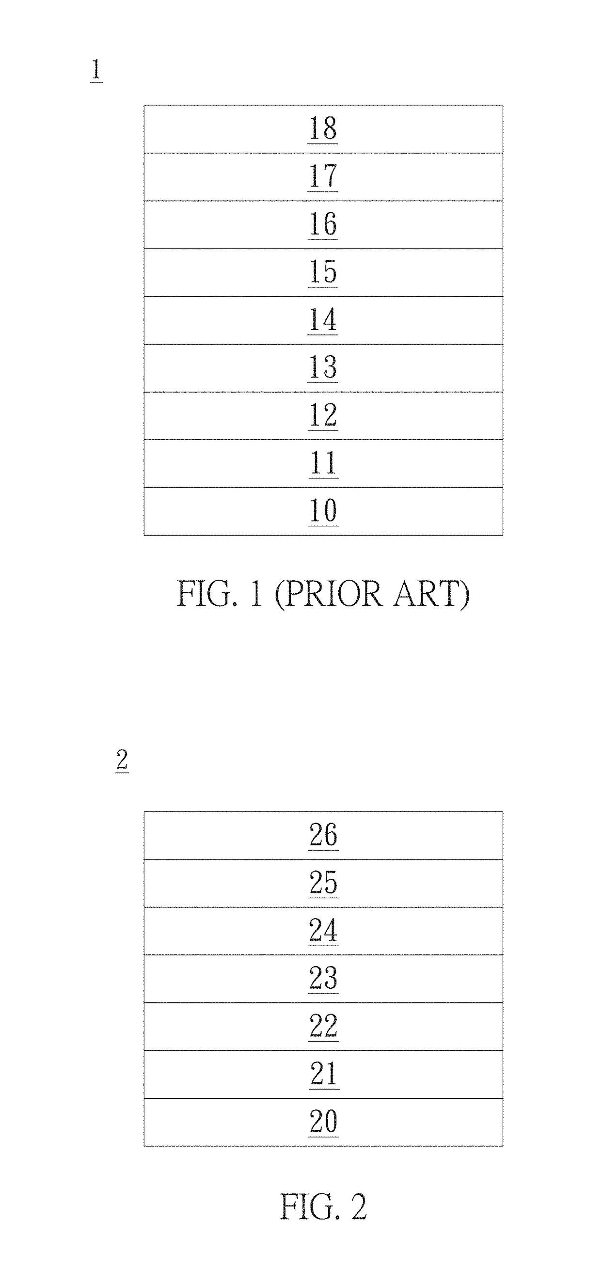
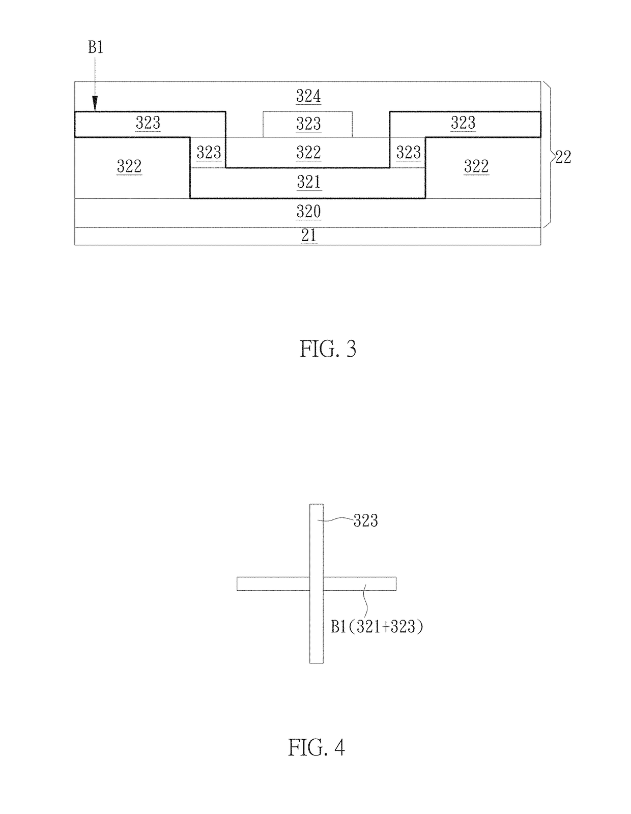
[0063]A preferred embodiment of the invention is an in-cell capacitive touch panel. In practical applications, the in-cell capacitive touch panel can achieve thinnest touch panel design; therefore, it can be widely used in portable electronic products such as mobile phones, tablet PCs, and notebooks.

[0064]In this embodiment, the in-cell mutual-capacitive touch panel can be suitable for displays using in-plane switching liquid crystal (IPS) technology, fringe field switching (FFS) technology, or advanced hyper-viewing angle (AHVA) technology, but not limited to these cases.

[0065]In general, the most popular capacitive touch sensing technology in nowadays should be the projected capacitive touch sensing technology including a mutual-capacitive type and a self-capacitive type. As to the mutual-capacitive touch sensing technology, when a touch occurs, capacitive coupling will be generated between two electrode layers adjacent to the touch point, and the capacitance change between the tw...


PUM

PropertyMeasurementUnit
conductiveaaaaaaaaaa
light resistanceaaaaaaaaaa
floating voltageaaaaaaaaaa

Abstract

An in-cell touch panel and its trace layout are disclosed. The in-cell touch panel includes a plurality of pixels. Each pixel has a laminated structure bottom-up including a substrate, a TFT layer, a liquid crystal layer, a color filter layer, and a glass layer. The TFT layer is disposed on the substrate. A first conductive layer and a second conductive layer are integrated in the TFT layer. The liquid crystal layer is disposed on the TFT layer. The color filter layer is disposed on the liquid crystal layer. The glass layer is disposed on the color filter layer. The design of touch sensing electrodes and their trace layout in the in-cell touch panel of the application is simple and it can effectively reduce cost and reduce the RC loading of a common electrode.

Description

BACKGROUND OF THE INVENTION[0001]Field of the Invention[0002]This invention relates to a touch panel, especially to an in-cell touch panel and trace layout thereof.[0003]Description of the Related Art[0004]Please refer to FIG. 1. FIG. 1 illustrates a laminated structure of a conventional on-cell capacitive touch panel. As shown in FIG. 1, the laminated structure 1 of the conventional on-cell capacitive touch panel includes a substrate 10, a thin-film transistor layer 11, a liquid crystal layer 12, a color filtering layer 13, a glass layer 14, a touch sensing layer 15, a polarizer 16, an adhesive 17, and top lens 18.[0005]From FIG. 1, it can be found that the touch sensing layer 15 of the on-cell capacitive touch panel is disposed above the glass layer 14; that is to say, the touch sensing layer 15 is disposed out of the liquid crystal display module of the on-cell capacitive touch panel. Compared to the conventional one glass solution (OGS), the on-cell capacitive touch panel can ac...

Claims


Application Information

Patent Timeline
Patent Type & Authority Patents(United States)
IPC IPC(8): G06F3/044G02F1/1335G02F1/1368G06F3/041G02F1/1333
CPCG06F3/044G02F1/1368G06F3/0412G02F1/133512G02F1/133514G02F1/13338G02F1/134363G06F3/0443G06F3/0446
Inventor LEE, KUN-PEILIN, YI-YINGCHIANG, CHANG-CHING
Owner RAYDIUM SEMICON
Why Eureka
Try Eureka