Thin-film transistor array substrate and liquid crystal display panel

一种液晶显示面板、薄膜晶体管的技术,应用在电固体器件、半导体器件、半导体/固态器件测试/测量等方向,能够解决影响液晶显示面板显示效果、液晶显示面板显示效果不佳、RC负载大等问题,达到提高显示品质、重叠面积减小、减小RC负载的效果

Active Publication Date: 2016-02-10
TCL CHINA STAR OPTOELECTRONICS TECH CO LTD +1
View PDF4 Cites 1 Cited by
  • Summary
  • Abstract
  • Description
  • Claims
  • Application Information

AI Technical Summary

Problems solved by technology

At the same time, since there is resistance among the sensing lines, gate lines, data lines and the common electrode layer of the sensing electrodes, the resistance-capacitance (RC) load of the pixel is relatively large, thereby affecting the display of the entire liquid crystal display panel. Effect
To sum up, in the prior art, the RC load of the pixel is relatively large, and the display effect of the entire liquid crystal display panel is not good.

Method used


Image

  • Thin-film transistor array substrate and liquid crystal display panel
  • Thin-film transistor array substrate and liquid crystal display panel
  • Thin-film transistor array substrate and liquid crystal display panel

Examples


Embodiment Construction

[0028] The following will clearly and completely describe the technical solutions in the embodiments of the present invention with reference to the accompanying drawings in the embodiments of the present invention. Obviously, the described embodiments are only some, not all, embodiments of the present invention. Based on the embodiments of the present invention, all other embodiments obtained by persons of ordinary skill in the art without making creative efforts belong to the protection scope of the present invention.

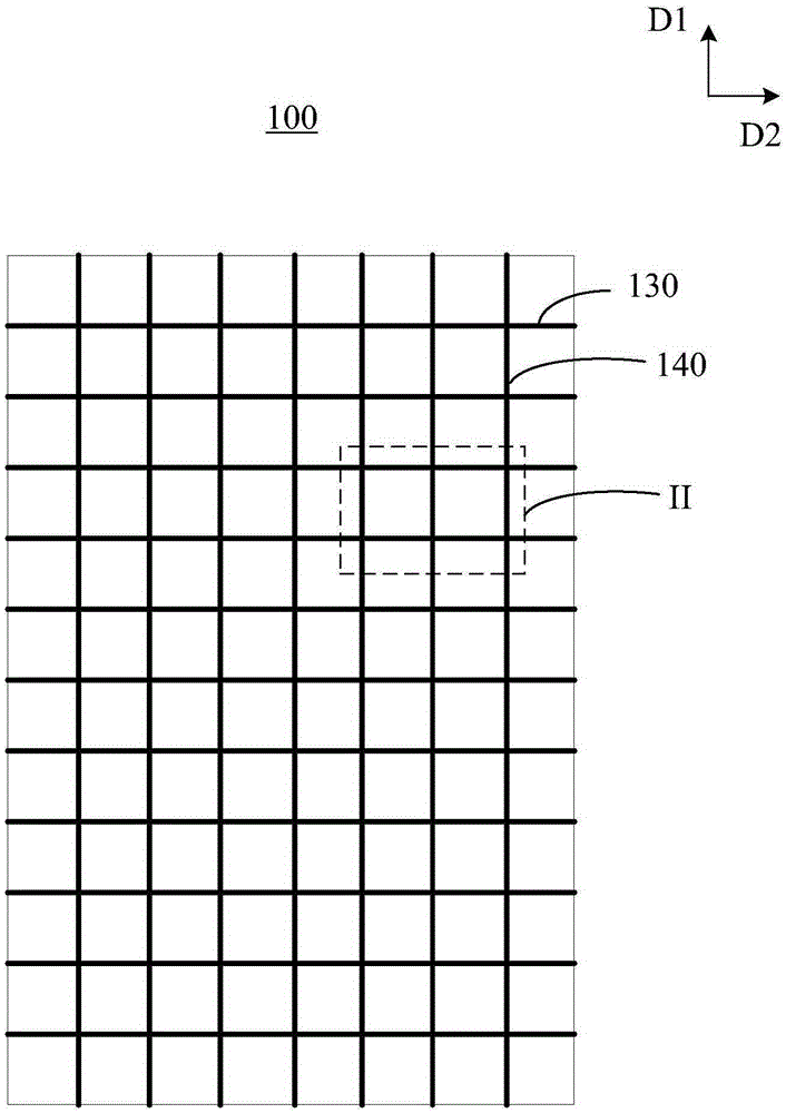
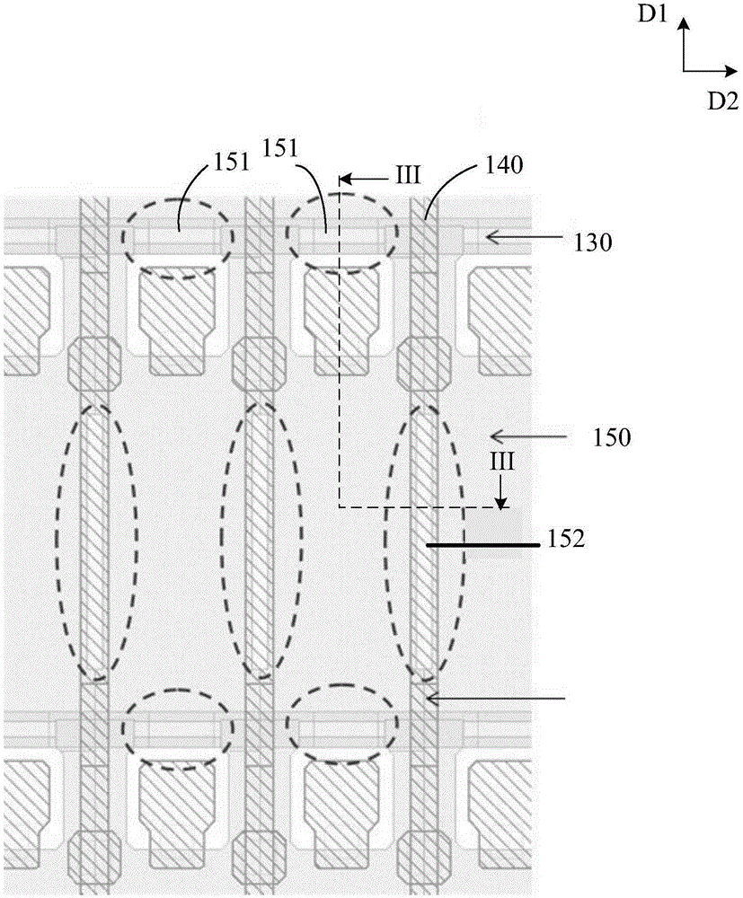
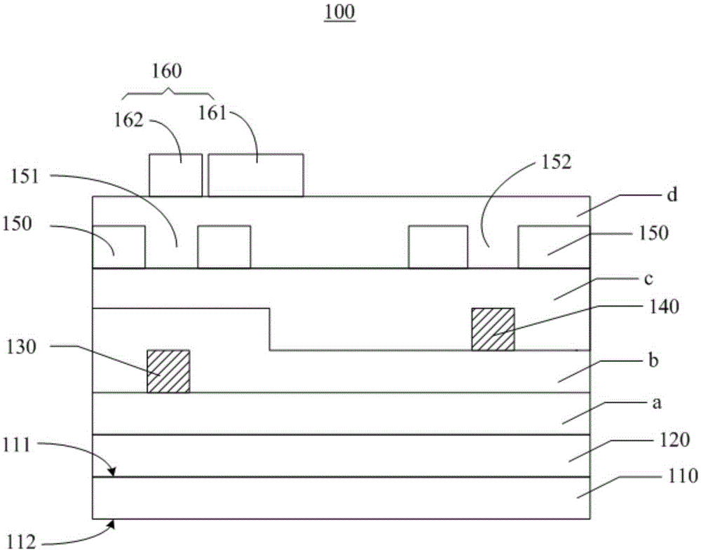
[0029] Please also refer to figure 1 , figure 2 and image 3 , figure 1 It is a structural schematic diagram of a thin film transistor array substrate according to a preferred embodiment of the present invention; figure 2 for the invention figure 1 Schematic diagram of the enlarged structure at II; image 3 for the invention figure 2 Schematic diagram of the cross-sectional structure of III-III. The TFT array substrate 100 includes a substrate 110 , ...


PUM


Abstract

The invention provides a thin-film transistor array substrate and a liquid crystal display panel. The thin-film transistor array substrate comprises a substrate, a thin-film transistor array, a common electrode layer and a sensing electrode layer, wherein the substrate comprises a first surface and a second surface, which are oppositely arranged; the thin-film transistor array is arranged on the first surface; the common electrode layer and the thin-film transistor array are arranged in an insulating manner; the common electrode comprises a plurality of first strip holes; the sensing electrode layer and the common electrode layer are arranged in the insulating manner; the sensing electrode layer comprises a plurality of sensing units and a plurality of sensing lines; the sensing units are arranged in rows and columns; the sensing lines are electrically connected with each row or each column of sensing units respectively; and the sensing lines are arranged correspondingly to the first strip holes.

Description

technical field [0001] The invention relates to the field of liquid crystal display, in particular to a thin film transistor array substrate and a liquid crystal display panel. Background technique [0002] A liquid crystal display panel (Liquid Crystal Display, LCD) is a common electronic device, and is favored by users because of its low power consumption, small size, and light weight. The integration of touch display is also known as a hotspot along the display panel research, and low temperature polysilicon (LowTemperaturePoly-silicon, LTPS) incell technology is regarded as a high-end technology in this field. The so-called incell technology refers to embedding the touch panel function into the liquid crystal pixel (Pixel). In the traditional pixel design process, there is a relatively large overlapping area between the sensing traces, gate lines, and data lines of the sensing electrodes and the common electrode layer. Therefore, the sensing electrodes of the sensing el...

Claims


Application Information

Patent Timeline
Patent Type & Authority Applications(China)
IPC IPC(8): H01L27/12H01L21/66G02F1/1362G02F1/1368
CPCG02F1/136286G02F1/1368H01L22/32H01L27/124G02F1/13338G06F3/0412G02F1/1333G06F3/0445G06F3/0446G02F2201/121G06F3/041G02F1/13606
Inventor 陈归陈彩琴
Owner TCL CHINA STAR OPTOELECTRONICS TECH CO LTD
Why Eureka
Try Eureka