Organic light-emitting display panel and forming method thereof

a technology of light-emitting display panels and organic materials, applied in the direction of basic electric elements, electrical apparatus, semiconductor devices, etc., can solve the problems of black specks, easy deformation or invalidation of the property of the oled device, and the thickness of the device as a whole, so as to achieve the effect of decreasing the frame region

Active Publication Date: 2016-12-15
WUHAN TIANMA MICRO ELECTRONICS CO LTD +1
View PDF5 Cites 36 Cited by
  • Summary
  • Abstract
  • Description
  • Claims
  • Application Information

AI Technical Summary

Benefits of technology

[0014]With the organic light-emitting display panel and the method for forming an organic light-emitting display panel provided in the present disclosure, since the block pole is disposed at the periphery of the organic light-emitting structure, it can be achieved that the package layer effectively covers the organic light-emitting structure. In addition, if a narrow-frame design is desired for packaging, the block pole can be disposed at a position close to the edge of the organic light-emitting structure as soon as possible, thereby decreasing the frame regions of the organic light-emitting display panel that are not light-emitted to realize the narrow-frame design.

Problems solved by technology

As for an organic electronic device, in particular the OLED, it is not desired for oxygen and moisture from the ambient to enter into inside of the device to contact the sensitive organic medium and electrodes.
That is because the property of the OLED device is easily degraded or invalidated due to the existence of the oxygen and moisture inside the OLED device, and even a tiny amount of moisture will cause an organic compound layer and an electrode layer to be peeled off, thereby producing a black speck.
However, the sealed case has a relative large quality such that the whole dimension of the device is thickened accordingly, which in not in conformity with the light and thin requirements.
In addition, the metal is also not suitable for some application due to its opaqueness.
The material of the organic film layer has s worse performance of blocking water and oxygen, and cannot be directly exposed in the air.
1. Although it is guaranteed that the organic film layer is entirely covered inside the non-organic firm layer by enlarging the design value of the coverage area of the non-organic firm layer, the existence of an extended region will lead to an increase in the coverage area of the non-organic firm layer. In addition, the non-organic firm layer itself has a certain extended effect, so that an invalid region located at the periphery of the device is enlarged ultimately, thereby it is not advantageous to a design of narrow frame of the organic electroluminescence.
2. The material of the organic firm layer has a low capability of blocking water and oxygen, even has a capability of absorbing water and oxygen. In terms of the package design of the thin film, it is required that the non-organic firm layer has a coverage area larger than a coverage area of the organic firm layer. However, the precursor of the organic firm layer is generally formed by a liquid material, and the flow of the liquid material is uncontrollable in a certain degree, the extended length of any of positions located at the periphery of the device are not all same as each other, and the fluctuation of the distribution strengths when the thickness of the organic firm layer becomes larger and larger. It is not guaranteed that the organic firm layer is covered efficiently only by relying on the fixed design value of the non-organic firm layer, and the requirement of blocking water and oxygen of the electroluminescence device is unreachable.

Method used


Image

  • Organic light-emitting display panel and forming method thereof
  • Organic light-emitting display panel and forming method thereof
  • Organic light-emitting display panel and forming method thereof

Examples


Embodiment Construction

[0025]In order to better explain the technical contents of the present disclosure, the disclosure will be further described below by example of specific embodiments in combination with the accompanying drawings. The invention is not limited to the specific embodiments and accompanying drawings. For those skilled in the art, changes and modifications can be made to the present disclosure without departing from the spirit and principle of the present disclosure, the scope of the present disclosure should be defined by appended claims.

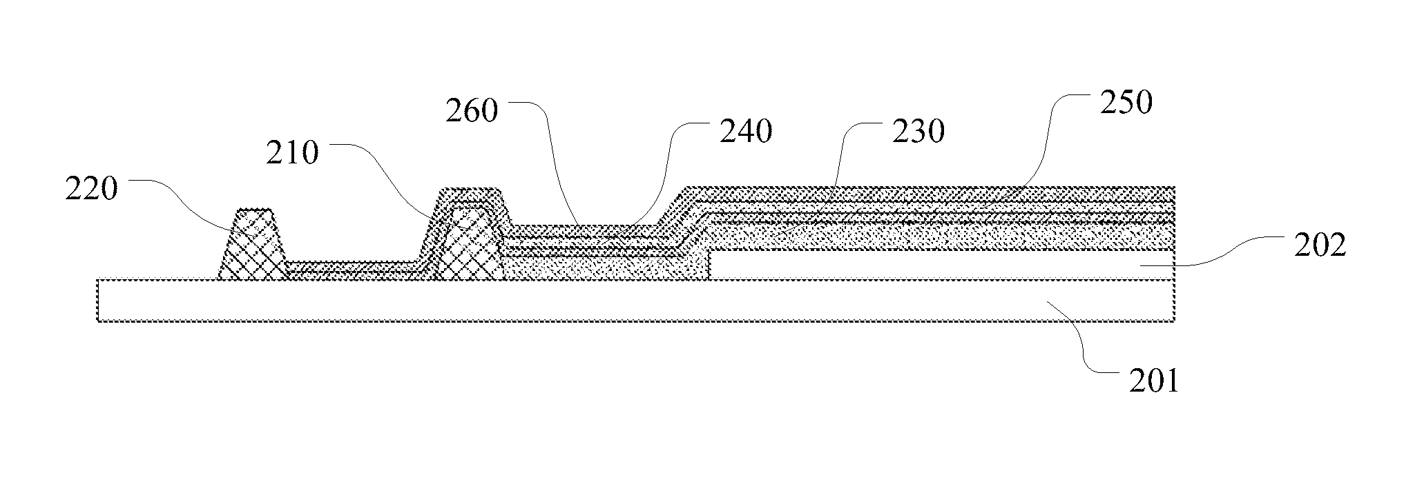
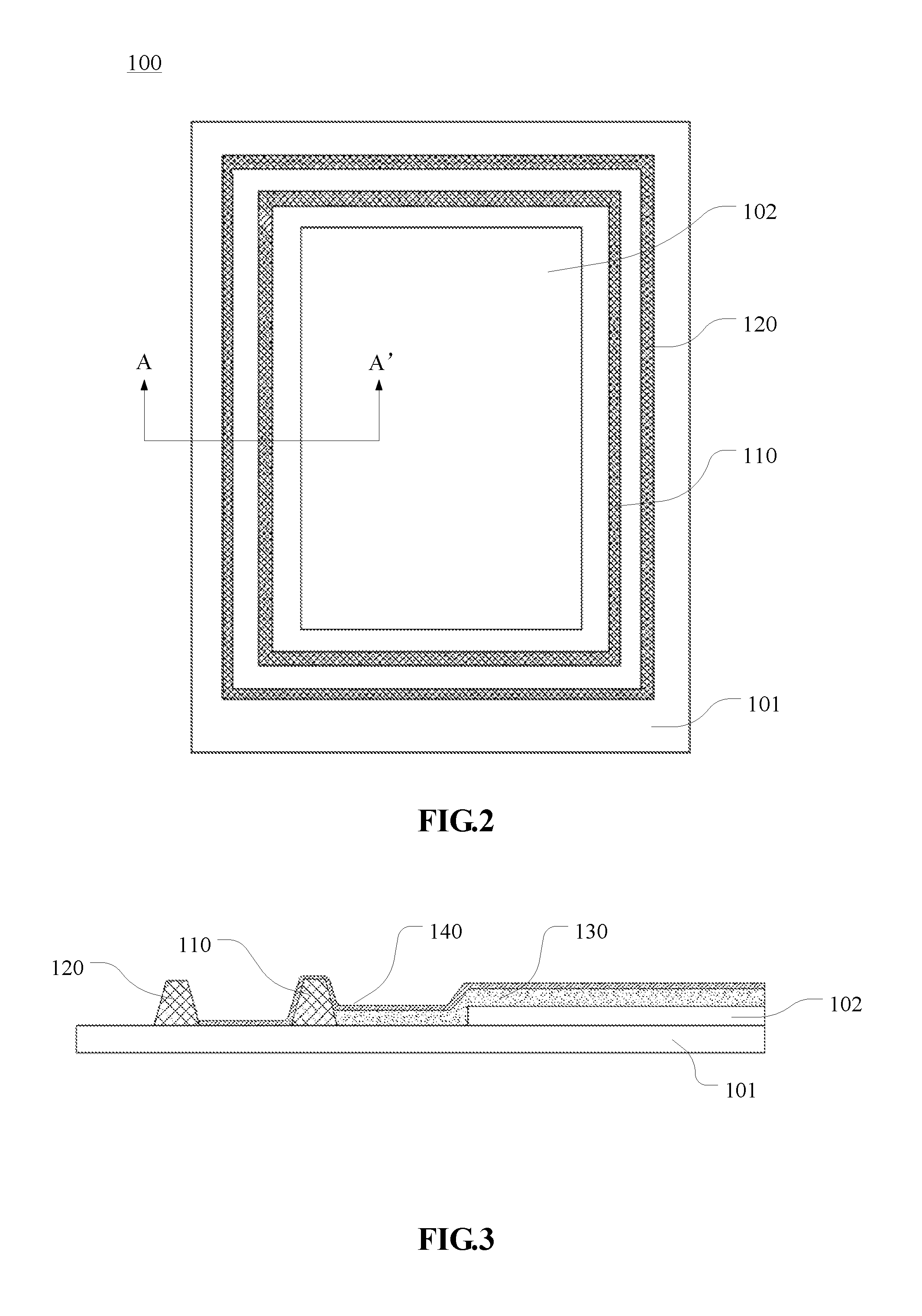
[0026]According to an embodiment of the present disclosure, an organic light-emitting display panel includes a substrate, an organic light-emitting structure disposed on the substrate, a package layer covering the organic light-emitting structure and a block pole disposed at the periphery of the organic light-emitting structure. The package layer can include at least one non-organic block layer and at least one organic block layer spaced apart from the at...


PUM


Abstract

The present disclosure provides an organic light-emitting display panel. The organic display panel comprises a substrate, an organic light-emitting structure disposed on the substrate, a package layer covering the organic light-emitting structure. The package layer comprises at least one non-organic block layer and at least one organic block layer, and a block pole. The block pole comprises a first block pole and a second block pole. The second block pole is disposed at the periphery of the first block pole. The at least one non-organic block layer comprises an outmost non-organic block layer. The first block pole is at least covered by the outmost non-organic block layer. The at least one organic block layer can partially cover the first block pole or not cover the first block pole at all. The at least one non-organic block layer can partially cover the second block pole or not cover the second block pole at all.

Description

CROSS-REFERENCES TO RELATED APPLICATIONS[0001]This application claims priority to a Chinese patent application No. 201510314150.4 filed on Jun. 9, 2015 and entitled “Organic Light-emitting Display Panel and Forming Method Thereof”, the disclosure of which is incorporated herein by reference in its entirety.TECHNICAL FIELD[0002]The present disclosure relates to the field of organic electroluminescence display technologies, in particular to an organic light-emitting display panel and a forming method thereof.TECHNICAL BACKGROUND[0003]Recently, an organic light-emitting display panel used as a flat panel display, which is a light-emitting device itself, is greatly concerned by more and more people. The organic light-emitting display panel is realized through an Organic Light-Emitting Diode (OLED) disposed on a substrate. The lifetime of the OLED device is not only dependent on selected organic material but it is also dependent on a method for packing the device. As for an organic elect...

Claims


Application Information

Patent Timeline
Patent Type & Authority Applications(United States)
IPC IPC(8): H01L27/32H01L51/56H01L51/52
CPCH01L27/3244H01L51/5256H01L51/5246H01L2227/323H01L51/5253H01L51/56H01L51/525H10K50/8426H10K59/12H10K50/844H10K50/8428H10K50/8445H10K71/00H10K59/1201
Inventor XU, ZHAOZHEFANG, JUNXIONG
Owner WUHAN TIANMA MICRO ELECTRONICS CO LTD
Why Eureka
Try Eureka