Semiconductor device having input/output line drive circuit and semiconductor system including the same

Active Publication Date: 2017-02-02
SK HYNIX INC
View PDF10 Cites 2 Cited by
  • Summary
  • Abstract
  • Description
  • Claims
  • Application Information

AI Technical Summary

Benefits of technology

The patent describes semiconductor devices and systems with improved input / output line drive circuits and refresh operations. The systems include a first semiconductor device that outputs a command / address signal and a second semiconductor device that extracts an active signal, pre-charge signals, and addresses from the command / address signal. The first semiconductor device also includes an input buffer, a first coupling unit, a second coupling unit, a refresh control unit, a memory portion, and a select transmission unit. The second semiconductor device includes an input buffer, a signal generating unit, a counter, a latch control signal, and a select transmission unit. The systems allow for efficient refreshing and operation of memory cells.

Problems solved by technology

Unlike static random access memory (SRAM) devices or flash memory devices, the DRAM devices may lose data stored in their memory cells as time elapses.

Method used


Image

  • Semiconductor device having input/output line drive circuit and semiconductor system including the same
  • Semiconductor device having input/output line drive circuit and semiconductor system including the same
  • Semiconductor device having input/output line drive circuit and semiconductor system including the same

Examples


Embodiment Construction

[0046]Various embodiments of the present disclosure will be described hereinafter with reference to the accompanying drawings. However, the embodiments described herein are for illustrative purposes only and are not intended to limit the scope of the present disclosure.

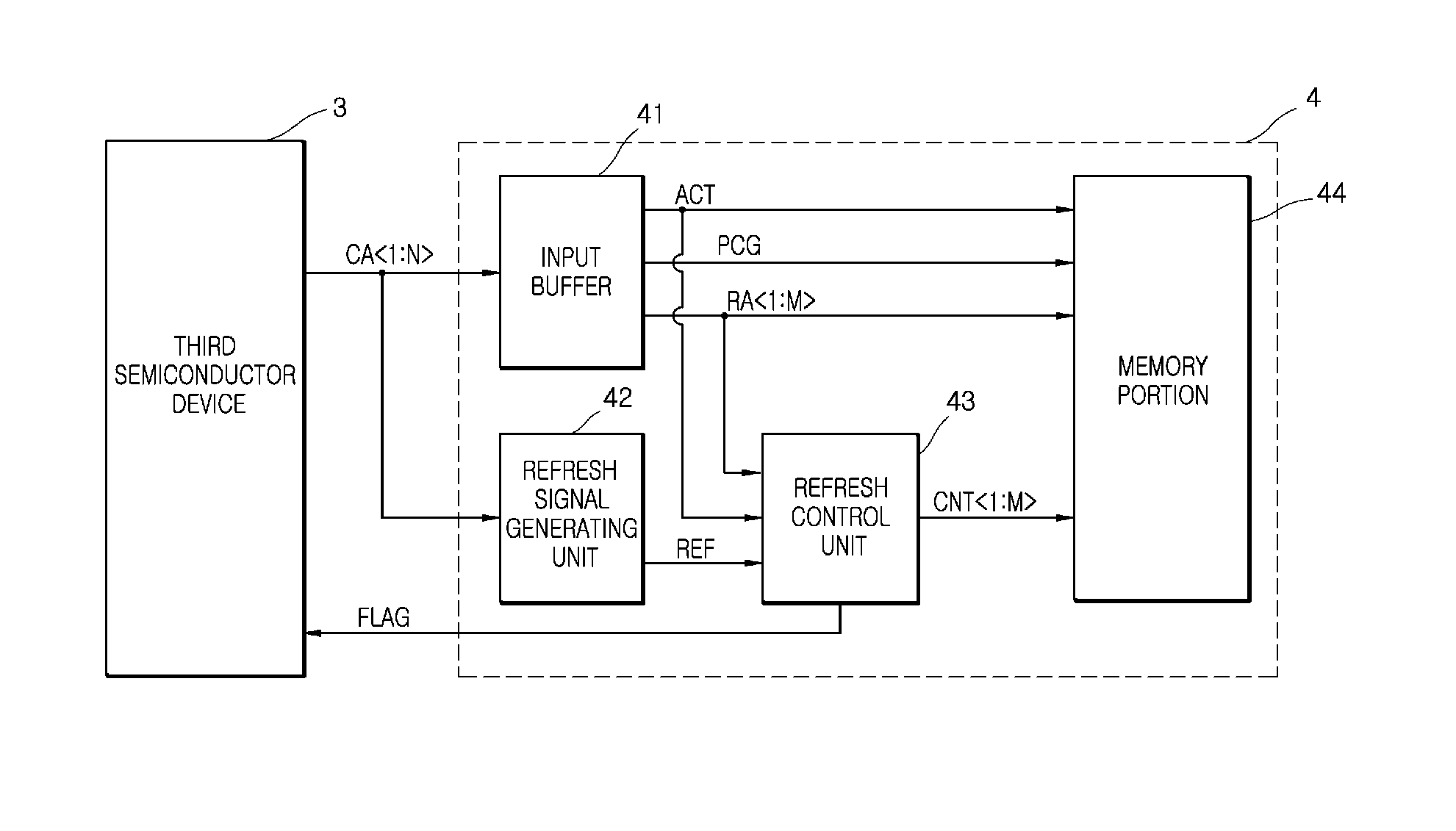
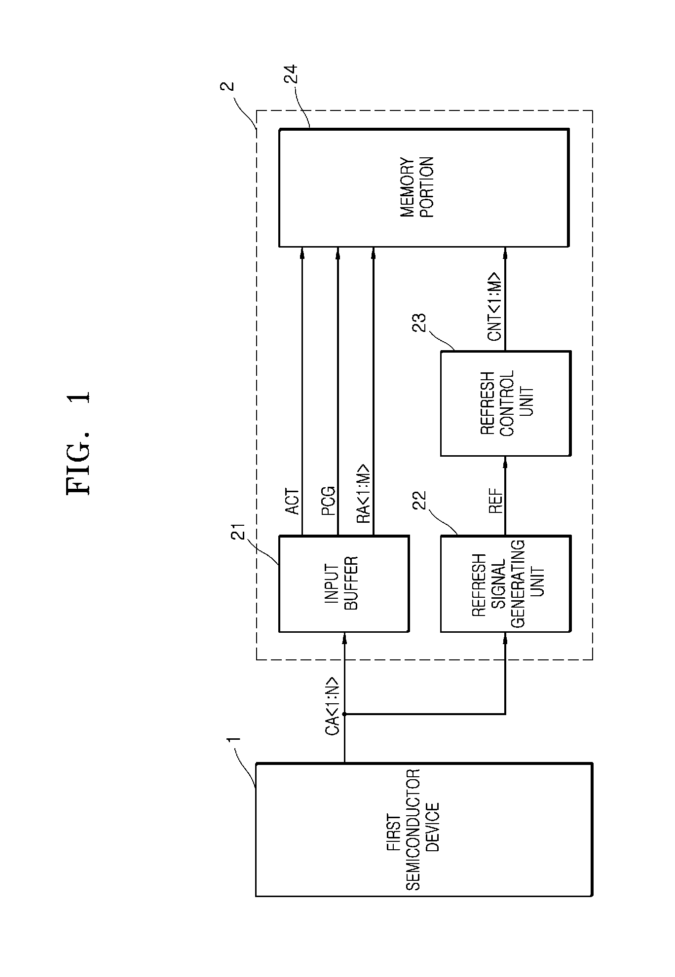
[0047]As illustrated in FIG. 1, a semiconductor system according to an embodiment of the present disclosure may include a first semiconductor device 1 and a second semiconductor device 2. The second semiconductor device 2 may include an input buffer 21, a refresh signal generating unit 22, a refresh control unit 23, and a memory portion 24.

[0048]The first semiconductor device 1 may output command / address signals CA. The command / address signals CA may be transmitted through signal lines. Addresses, commands, and data signals may be transmitted through separate signal lines. Alternatively, the command / address signals CA may be sequentially transmitted through a single line. The number of bits in the command / address sign...


PUM


Abstract

A semiconductor system includes a first semiconductor device and a second semiconductor device. The first semiconductor device outputs a command / address signal. The second semiconductor device extracts an active signal, a pre-charge signal, and addresses from the command / address signal, performs an active operation on a memory cell corresponding to the addresses, and performs a refresh operation on the memory cell corresponding to counting signals generated by counting a number of pulses in a refresh signal.

Description

CROSS-REFERENCE TO RELATED APPLICATIONS[0001]The present application claims priority under 35 U.S.C. 119(a) to Korean Patent Application No. 10-2015-0106091 filed on Jul. 27, 2015, in the Korean Intellectual Property Office, which is incorporated herein by reference in its entirety.BACKGROUND[0002]1. Technical Field[0003]Embodiments of the present disclosure generally relate an integrated circuit, and more particularly to semiconductor device having an input / output (I / O) line drive circuit that performs an active operation during a refresh operation in accordance with a command / address signal and semiconductor systems including the semiconductor devices.[0004]2. Related Art[0005]A semiconductor memory device may include word lines, bit lines, and memory cells coupled the word lines and the bit lines. When the semiconductor memory device stores data in the memory cells and outputs the data stored in the memory cells, the word lines and the bit lines are used. That is, the semiconduct...

Claims


Application Information

Patent Timeline
IPC IPC(8): G11C11/408G11C11/4093G11C11/4094G11C11/406G11C11/4091
CPCG11C11/4085G11C11/406G11C11/4087G11C11/4094G11C11/4093G11C11/4091G11C11/40603G11C11/40618
Inventor PARK, MIN SU
Owner SK HYNIX INC
Why Eureka
Try Eureka