Microelectromechanical system and fabricating process

a technology of microelectromechanical systems and fabricating processes, applied in the direction of fluid speed measurement, instrumentation, and semiconductor/solid-state device details, etc., can solve the problems of slow stress variation, output signal of sensors to drift, and inability to compensate for dri

Active Publication Date: 2017-04-20
THALES SA
View PDF7 Cites 9 Cited by
  • Summary
  • Abstract
  • Description
  • Claims
  • Application Information

AI Technical Summary

Benefits of technology

The technical effect of this patent is to create a device that can be attached to another object without transmitting too much force or stress between them. This helps protect the delicate components within the device while still attaching it securely.

Problems solved by technology

The technical problem addressed in this patent is the need to limit the transmission of thermomechanical stresses to the sensitive structure of a MEMS sensor, which can cause drift in the sensor's output signal. The patent proposes the use of a flexible decoupling structure to filter out the deformation of the carrier in order to minimize the transmission of mechanical stresses. However, the current solutions are limited by the need for a hyperstatic fastening structure, which can still transmit some of the deformation to the sensor.

Method used


Image

  • Microelectromechanical system and fabricating process
  • Microelectromechanical system and fabricating process
  • Microelectromechanical system and fabricating process

Examples


Embodiment Construction

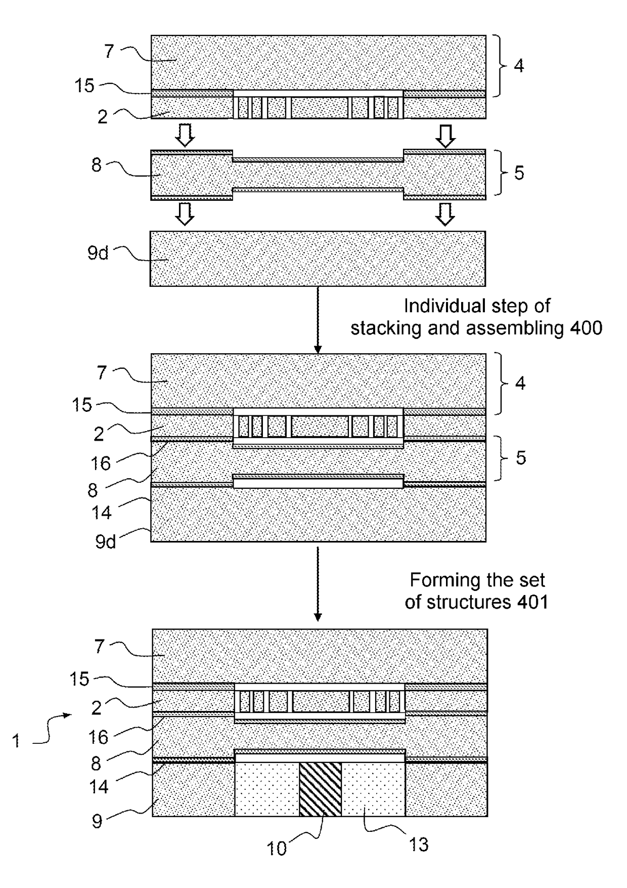
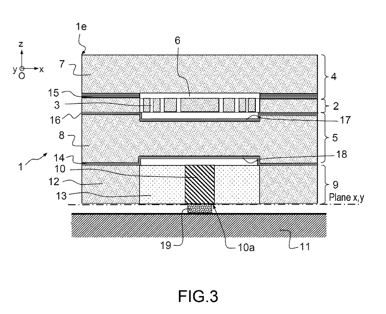
[0058]FIG. 3 schematically shows a cross-sectional view of a microelectromechanical system or MEMS chip according to the invention. The cross section is produced in a plane comprising the stacking direction z.

[0059]The microsystem according to the invention is for example a sensor.

[0060]As may be seen in FIG. 3, the microelectromechanical system 1 or MEMS chip according to the invention comprises an assembly 1e of a plurality of layers stacked in the stacking direction z. The plurality of layers comprises:

[0061]a single-crystal silicon active layer 2, said active layer 2 comprising an active structure 3 of the microelectromechanical system 1, and

[0062]a first cover 4 and a second cover 5 defining a cavity 6 around the active structure 3.

[0063]The active structure 3 is micro-machined in the plane of the silicon layer 2. The active structure is a structure that is able to move, i.e. able to deform freely, with respect to the rest of the active layer 2 and more particularly with respec...


PUM

PropertyMeasurementUnit
Timeaaaaaaaaaa
Timeaaaaaaaaaa
Shapeaaaaaaaaaa

Abstract

A microelectromechanical system comprising an assembly of layers stacked in a stacking direction comprises an active layer made of single-crystal silicon comprising an active structure, and first and second covers defining a cavity around the active structure, the active layer interposed between the first and second covers, the second cover comprising a single layer made of single-crystal silicon. The assembly comprises a decoupling layer made of single-crystal silicon and comprising: an attaching element fastened to a carrier, a frame encircling the attaching element in the plane of the decoupling layer, and a mechanical decoupling structure connecting the frame and the attaching structure, the mechanical decoupling structure allowing the attaching element to be flexibly joined to the frame. The frame is secured to the silicon layer of the second cover and at most one film of silicon dioxide is interposed between the frame and silicon layer of the second cover.

Description


Claims


Application Information

Patent Timeline
Owner THALES SA
Why Eureka
Try Eureka