

Multi-loop pll structure for generating an accurate and stable frequency over a wide range of frequencies
- Summary
- Abstract
- Description
- Claims
- Application Information
AI Technical Summary
Benefits of technology
Problems solved by technology
Method used
Image

Examples
first embodiment
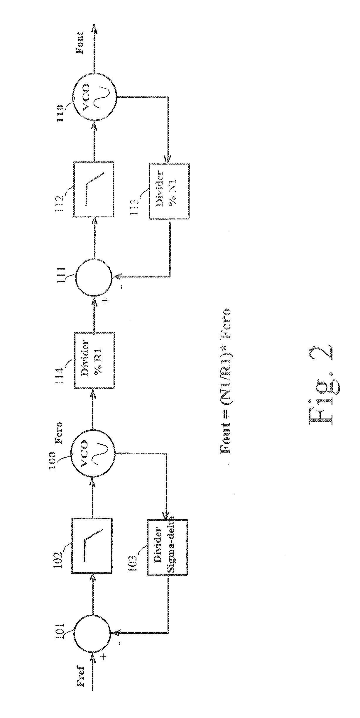
[0047]FIG. 2 illustrates one first embodiment of a dual loop PLL architecture which can use the configuration process which shall be described hereinafter.
[0048]The circuit comprises a first loop based on a first voltage controlled oscillator (VCO) 110 associated with a phase detector 111, a loop filter 112 and two dividers 113 and 114 having dividing ratios respectively equal to N1 and R1.
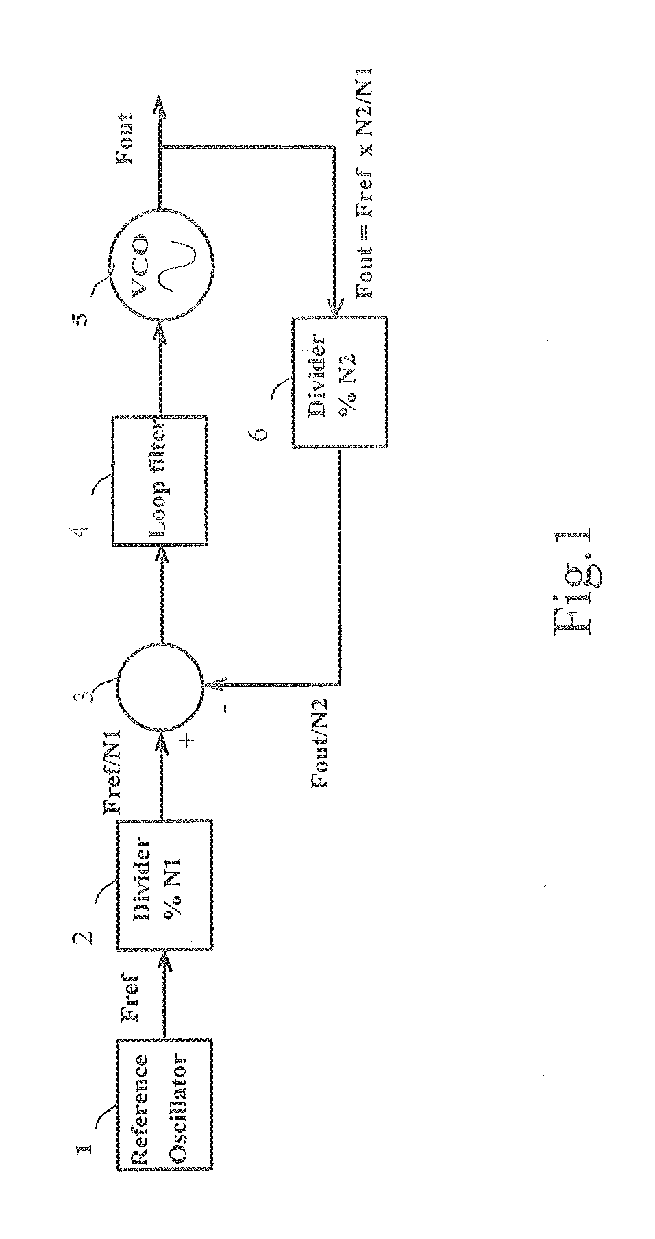
[0049]Divider 114 has an input and an output, the latter being connected to a first (non-inverting) input of phase detector 111 having a second inverting input receiving the output of divider block 113, the input of which is connected to receive the output frequency Fout of VCO 110. Phase detector 111 has an output which is connected to an input of a low pass filter 112, which output is further connected to the input of VCO 110, generating the output frequency Fout. Dividers 113 and 114 are configured to apply dividing ratios of N1 and R1, respectively.
[0050]The circuit of FIG. 2 further comprises...
second embodiment
[0062]Consequently, the second embodiment which was described above can be used for generating an output voltage having a frequency Fout such as:
Fout=(N1 / R1+N21R2)*Fcro
[0063]Where
[0064]N1 and R1 are the dividing ratios of blocks 213 and 214, respectively, and
[0065]N2 and R2 are the dividing ratios of blocks 223 and 224, respectively, and Fcro is the frequency generated by VCO 200.
[0066]One sees that the PLL architecture described in FIG. 3 significantly increases the level of redundancy of the frequency synthesis. Such level of redundancy is advantageously used for optimizing the frequency synthesis while taking into account a number of constraints: range of frequency for each VCO, accuracy of VCO oscillator 300 generating the frequency fcro.
[0067]In the preferred embodiment of FIG. 3, the following configuration is made to the different elements:
[0068]VCO 200 is a coaxial resonator oscillator which is an integrated oscillator associated with an appropriate LC resonator, which may ...
third embodiment
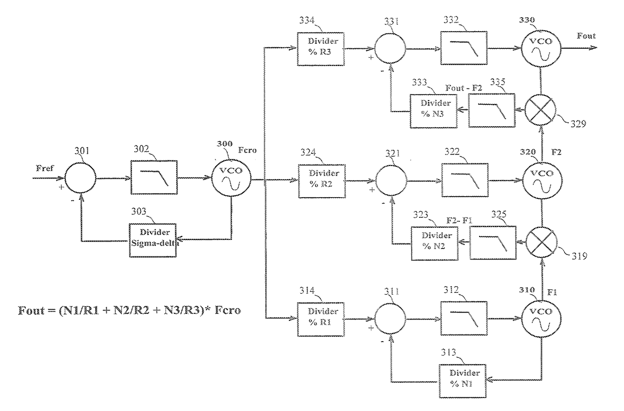
[0079]FIG. 4 shows a third embodiment which still increases the level of redundancy of the PLL multiloop architecture which is based on the use of four distinctive loops increasing the level of redundancy in the transfer function.[0080]The circuit of FIG. 4 comprises a first loop acting as a first auxiliary loop, based on a first voltage controlled oscillator (VCO) 310 associated with a phase detector 311, a loop filter 312 and two dividers 313 and 314, having dividing values being respectively equal to N1 and R1. Blocks 310-314 of FIG. 4 are similar to blocks 210-214 of FIG. 2. More particularly, divider 314 has an input and an output. The output of divider 314 is connected to a first (non-inverting) input of phase detector 311 having a second inverting input receiving the output of divider block 313, the input of which is connected to receive a first intermediate frequency F1 generated by VCO 310. Phase detector 311 has an output which is connected to an input of a low pass filter...
PUM
 Abstract
Description
Claims
Application Information