
Interposer with beyond reticle field conductor pads

a technology of conductor pads and interposers, which is applied in the field of interposers, can solve the problems of limiting the size and packing density of chips on conventional interposers, and the inability to place conductor pads and solder bumps overhangs,

Active Publication Date: 2017-07-27
ADVANCED MICRO DEVICES INC
View PDF0 Cites 31 Cited by
  • Summary
  • Abstract
  • Description
  • Claims
  • Application Information

AI Technical Summary

Benefits of technology

The present invention provides an apparatus that includes an interposer with two reticle fields and conductor pads on the first side. There are also dummy conductor pads on the first side in the second reticle field and outside the first reticle field. The invention also provides a semiconductor wafer with multiple interposers, each with conductor pads and dummy conductor pads on the first side in both reticle fields. A method of manufacturing is also provided that involves fabricating the conductor pads and dummy conductor pads on the interposer. The technical effects include improved performance and reliability of semiconductor devices, particularly in high-density packaging and advanced electronic applications.

Problems solved by technology

Stacked semiconductor chip devices present a host of design and integration challenges for scientists and engineers.
Common problems include providing adequate electrical interfaces between the stacked semiconductor chips themselves and between the individual chips and some type of circuit board, such as a motherboard or semiconductor chip package substrate, to which the semiconductor chips are mounted.
Still another technical challenge associated with stacked semiconductor chips is testing.
The overhang is unavailable for conductor pad and solder bump placement in conventional interposer fabrication.
This limits the sizes and packing density of chips on conventional interposers.

Method used


Image

  • Interposer with beyond reticle field conductor pads
  • Interposer with beyond reticle field conductor pads
  • Interposer with beyond reticle field conductor pads

Examples


Embodiment Construction

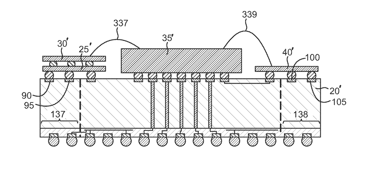
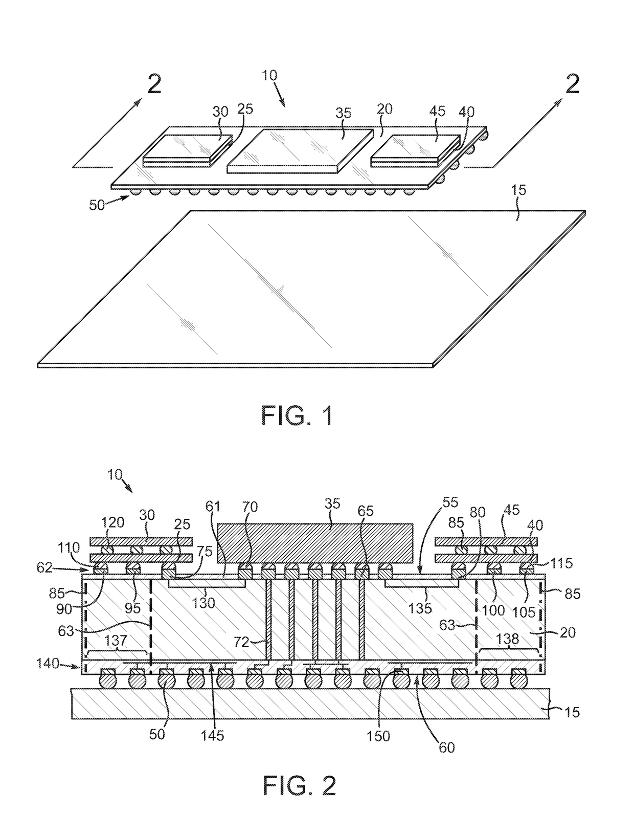
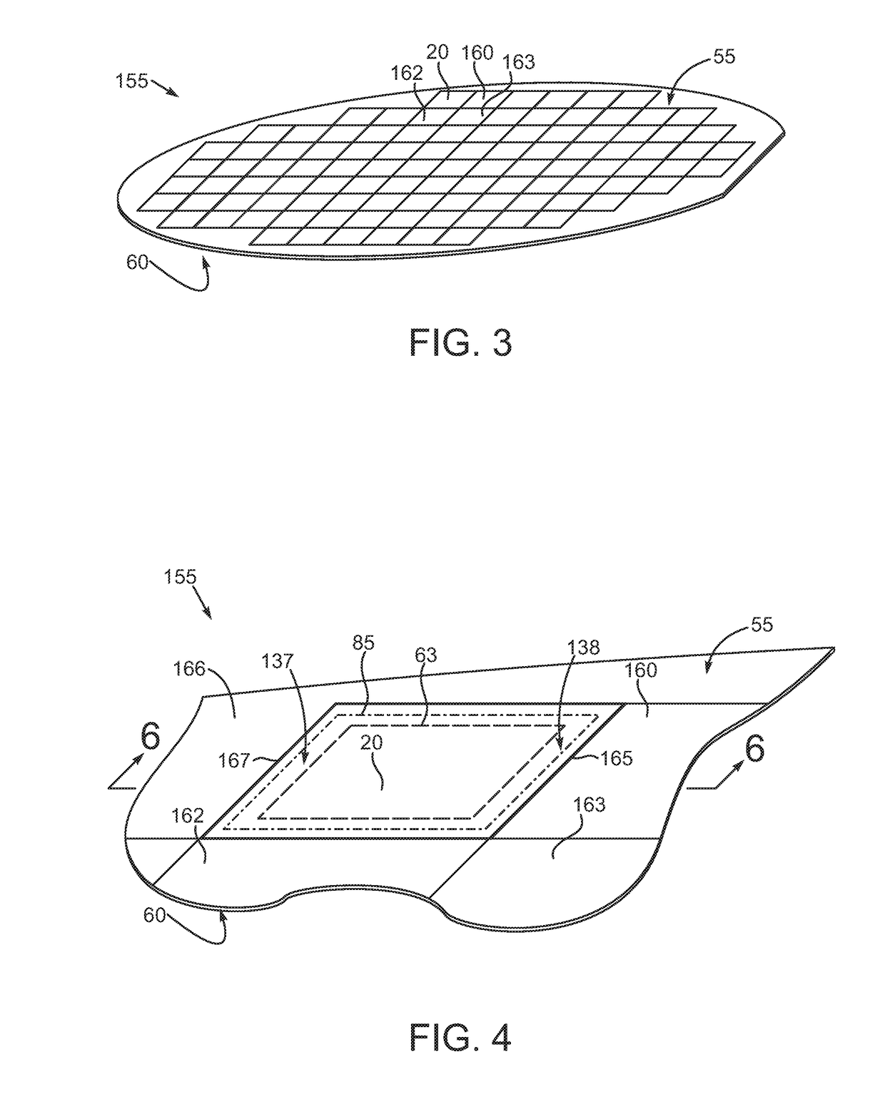
[0028]Various interposers useful for mounting multiple semiconductor chips are disclosed. The interposers include a first or top side and a second or bottom side. The top side includes a first reticle field and plural active conductor pads in the first reticle field. The top side includes a second reticle field that is larger than the first reticle field. There are plural dummy conductor pads in the second reticle field outside the first reticle field. The dummy electrical pads provide for solder bump and chip placement outside the smaller first reticle field. Additional details will now be described.

[0029]In the drawings described below, reference numerals are generally repeated where identical elements appear in more than one figure. Turning now to the drawings, and in particular to FIG. 1, therein is depicted a partially exploded pictorial view of an exemplary embodiment of a semiconductor chip device 10. The semiconductor chip device 10 may be mounted to a circuit board 15, whic...


PUM


Abstract

Various interposers and methods of manufacturing related thereto are disclosed. In one aspect, an apparatus is provided that includes an interposer that has a first side and a second side opposite the first side. The first side has a first reticle field and a second reticle field larger than the first reticle field. Plural conductor pads are positioned on the first side in the first reticle field. Plural dummy conductor pads are positioned on the first side in the second reticle field and outside the first reticle field.

Description

BACKGROUND OF THE INVENTION[0001]1. Field of the Invention[0002]This invention relates generally to semiconductor processing, and more particularly to interposers and methods of fabricating the same.[0003]2. Description of the Related Art[0004]Stacked semiconductor chip devices present a host of design and integration challenges for scientists and engineers. Common problems include providing adequate electrical interfaces between the stacked semiconductor chips themselves and between the individual chips and some type of circuit board, such as a motherboard or semiconductor chip package substrate, to which the semiconductor chips are mounted. Still another technical challenge associated with stacked semiconductor chips is testing.[0005]Semiconductor interposers are sometimes used to serve as supporting and interconnect substrates for one or more semiconductor chips. A conventional semiconductor interposer consists of a silicon substrate and metallization to provide electrical pathwa...

Claims


Application Information

Patent Timeline
Patent Type & Authority Applications(United States)
IPC IPC(8): H01L23/498H01L23/00H01L21/48
CPCH01L23/49838H01L21/4846H01L2224/16227H01L24/81H01L24/16H01L23/147H01L23/49816H01L23/49822H01L21/486H01L23/5384H01L2224/16145H01L2924/15192H01L2224/17181H01L2924/15311H01L2224/73257H01L2224/48137
Inventor ALFANO, MICHAEL S.BLACK, BRYANSU, MICHAEL Z.SIEGEL, JOSEPH R.DIN, JULIUS E.KASHEM, ANWAR
Owner ADVANCED MICRO DEVICES INC
Learn More