Integrated circuit device including vertical memory device and method of manufacturing the same

a technology of integrated circuits and memory devices, which is applied in the direction of semiconductor devices, semiconductor/solid-state device details, electrical apparatuses, etc., can solve the problems of complex, complicated, and inability to fully integrate the functions and features of the memory devices

Active Publication Date: 2017-08-03
SAMSUNG ELECTRONICS CO LTD
View PDF0 Cites 35 Cited by
  • Summary
  • Abstract
  • Description
  • Claims
  • Application Information

AI Technical Summary

Benefits of technology

[0004]According to an aspect of the inventive concept, there is provided an IC device including: a plurality of word lines that extend on a substrate parallel to a main surface of the substrate and are separated from one another in a first direction perpendicular to the main surface; a channel region that extends in a first region on the substrate through the plurality of word lines; a bit line contact pad that is on the channel region and contacts an upper surface of the channel region; a bit line that contacts the bit line contact pad in the first region and extends on the bit line contact pad in a second direction parallel to the main surface of the substrate; a common source line that partially fills a word line cut region, the word line cut region extending in a third direction on a side of the plurality of word lines, the third direction being parallel to the main surface of the substrate and intersecting the second direction, the common source line having a height lower than that of the channel region; and a common source via contact that contacts an upper surface of the common source line in the word line cut region and extends from the upper surface of the common source line in a direction away from the substrate.
[0005]According to another aspect of the inventive concept, there is provided an IC device including: a peripheral circuit on a substrate; a semiconductor layer on the peripheral circuit; a memory cell array region on the semiconductor layer and overlapping the peripheral circuit in a vertical direction, the memory cell array region including a plurality of memory cell arrays and a common source line tab region between adjacent two of the plurality of memory cell arrays; a plurality of word lines that extend on the semiconductor layer, parallel to a main surface of the substrate, and are included in each of the plurality of memory cell arrays and separated from one another in a first direction perpendicular to the main surface of the substrate; a plurality of channel regions that extend on the semiconductor layer in the first direction, passing through the plurality of word lines; a plurality of bit line contact pads that are on the plurality of channel regions to contact the plurality of channel regions; a plurality of bit lines that extend in a region separated from the common source line tab region, in a second direction parallel to the main surface of the substrate and contact a plurality of bit line contact pads; a common source line that partially fills a word line cut region, the word line cut region extending in a third direction on a side of the plurality of word lines, the third direction being parallel to the main surface of the substrate and intersecting the second direction, the common source line having a height lower than that of the plurality of channel regions; and at least one common source via contact that contacts an upper surface of the common source line in the common source line tab region and extends from the upper surface of the common source line in a direction away from the substrate.
[0006]According to another aspect of the inventive concept, there is provided a method of manufacturing an integrated circuit (IC) device, the method including forming a structure in which a plurality of insulating layers and a plurality of preliminary gate layers are alternately stacked one by one on a substrate. A plurality of channel holes penetrating the structure may be formed. A plurality of channel regions may be formed in a plurality of first channel

Problems solved by technology

The high integration of the memory devices with a reduction in memory cell sizes have made those functions and features included in the memo

Method used


Image

  • Integrated circuit device including vertical memory device and method of manufacturing the same
  • Integrated circuit device including vertical memory device and method of manufacturing the same
  • Integrated circuit device including vertical memory device and method of manufacturing the same

Examples


Embodiment Construction

[0022]Hereinafter, exemplary embodiments of the inventive concept will be described in detail with reference to the accompanying drawings. Like reference numerals in the drawings denote like elements, and thus their redundant description will be omitted.

[0023]It will be understood that, although the terms “first”, “second”, “third”, “fourth” etc. may be used herein to describe various elements, components, regions, layers and / or sections, these elements, components, regions, layers and / or sections should not be limited by these terms. These terms are only used to distinguish one element, component, region, layer or section from another element, component, region, layer or section. Thus, a first element, component, region, layer or section discussed below could be termed a second element, component, region, layer or section, or vice versa, without departing from the teachings of the present inventive concept.

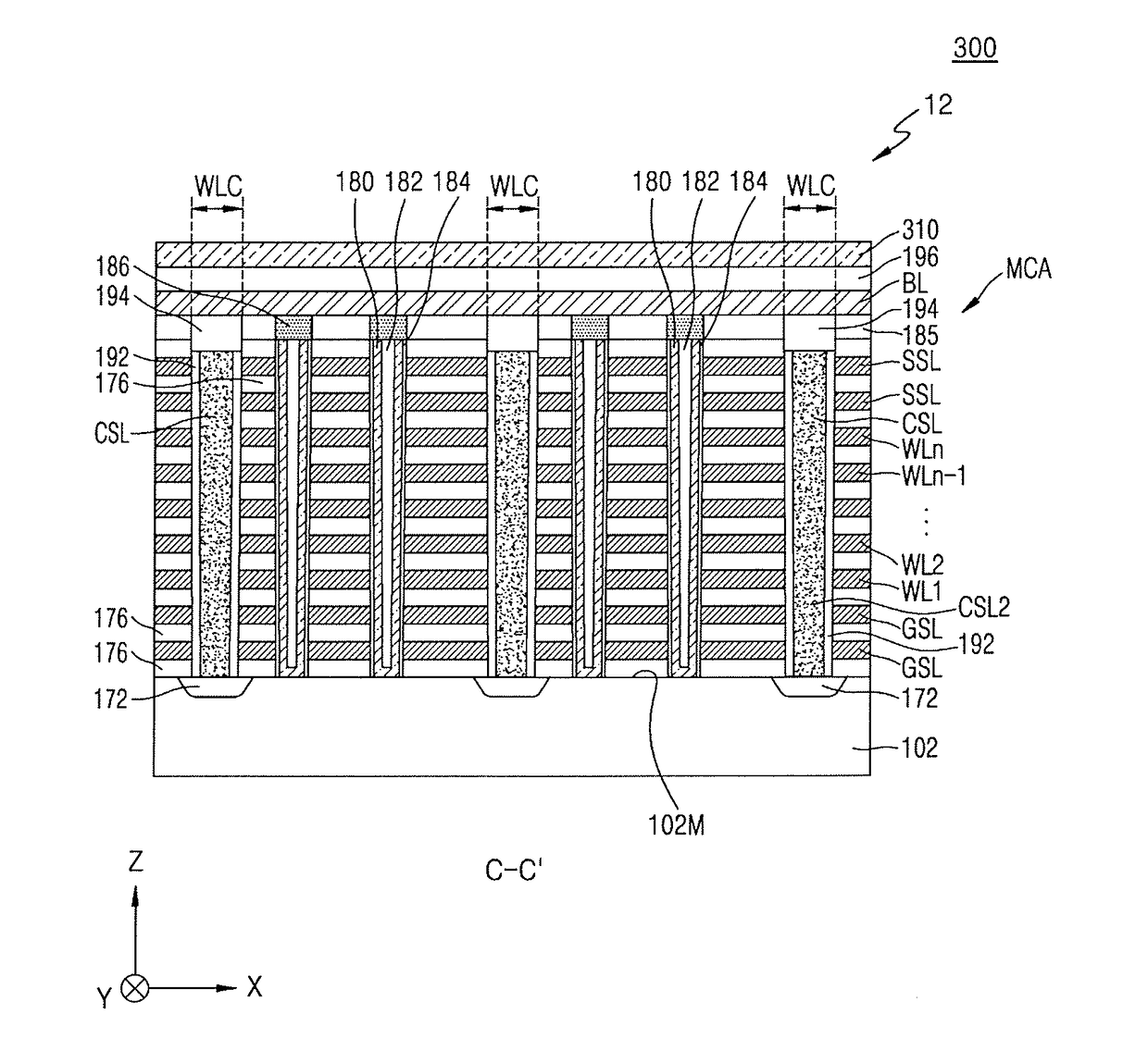
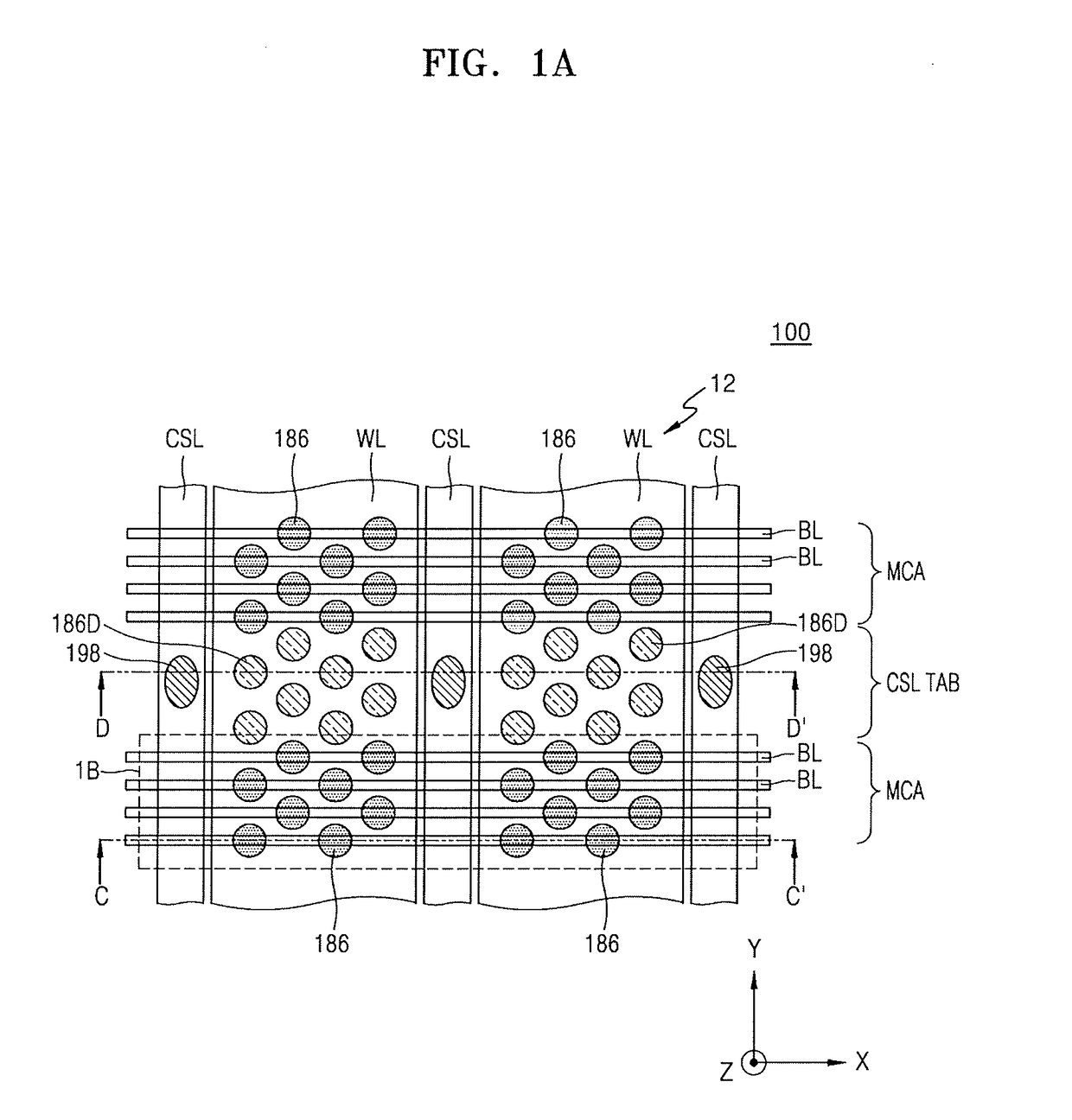
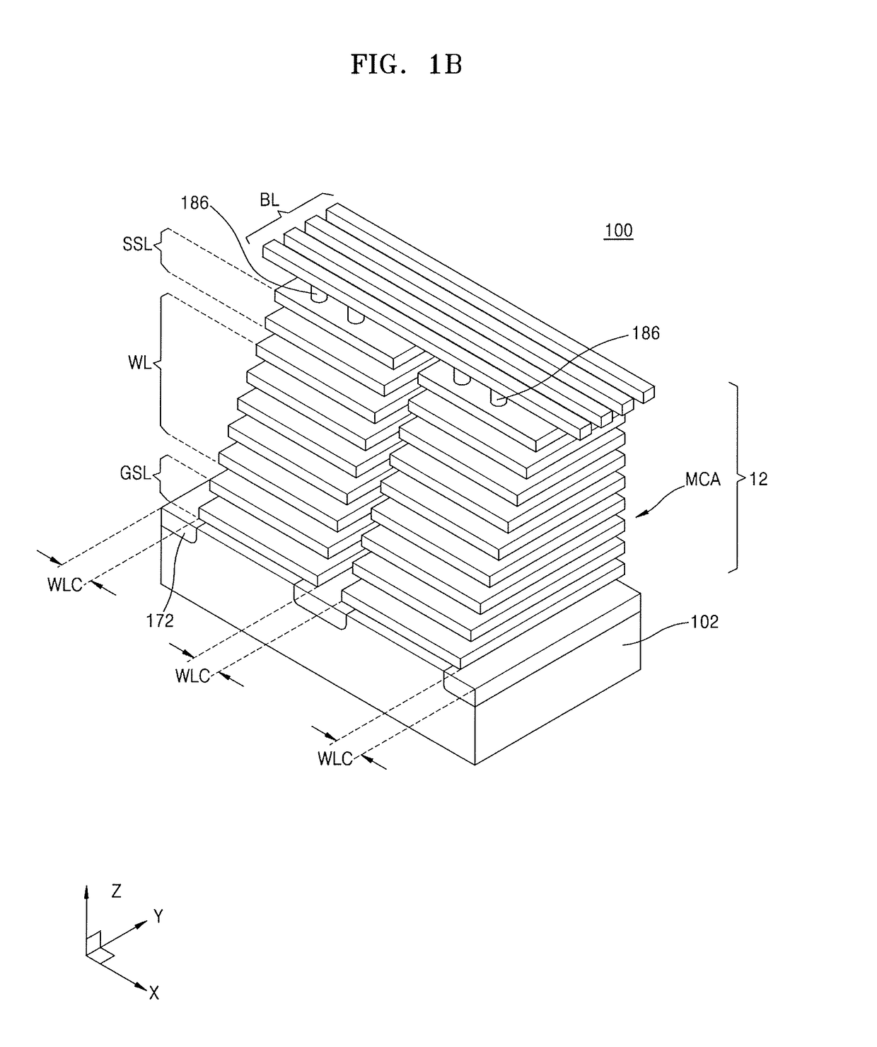
[0024]FIGS. 1A to 1D are views illustrating an integrated circuit (IC) devic...


PUM


Abstract

An integrated circuit (IC) device includes: a channel region that extends on the substrate to penetrate a plurality of word lines; a bit line contact pad that contacts an upper surface of the channel region; a bit line that contacts the bit line contact pad and extends on the bit line contact pad in a direction parallel to the main surface of the substrate; a common source line that partially fills a word line cut region and has a height lower than that of the channel region; and a common source via contact that contacts an upper surface of the common source line in the word line cut region.

Description

CROSS-REFERENCE TO RELATED APPLICATION[0001]This application claims the benefit under 35 U.S.C. §119 of Korean Patent Application No. 10-2016-0010725, filed on Jan. 28, 2016, in the Korean Intellectual Property Office, the disclosure of which is incorporated by reference herein in its entirety.TECHNICAL FIELD[0002]The inventive concept relates to an integrated circuit (IC) device and a method of manufacturing the IC device, and more particularly, to an IC device including a nonvolatile vertical memory device and a method of manufacturing the IC device.DISCUSSION OF RELATED ART[0003]Large capacity and high integration of IC devices including memory devices are features required to meet the demand for multifunctional information and communication devices. The high integration of the memory devices with a reduction in memory cell sizes have made those functions and features included in the memory devices such as operations of memory devices, and structures of operational circuits and i...

Claims


Application Information

Patent Timeline
IPC IPC(8): H01L23/522H01L27/115H01L23/528
CPCH01L23/5226H01L27/115H01L23/528H10B63/00H10B61/00H10B69/00H10K19/00H01L28/00H10B43/27
Inventor KIM, KWANG-SOO
Owner SAMSUNG ELECTRONICS CO LTD
Why Eureka
Try Eureka