Vertical memory devices and methods of manufacturing the same

a technology of vertical memory and manufacturing methods, applied in the direction of semiconductor devices, basic electric elements, electrical appliances, etc., can solve the problems of deteriorating the characteristics of memory devices, reducing the thickness of the layer,

Active Publication Date: 2017-08-03
SAMSUNG ELECTRONICS CO LTD
View PDF6 Cites 30 Cited by
  • Summary
  • Abstract
  • Description
  • Claims
  • Application Information

AI Technical Summary

Benefits of technology

[0006]In accordance with one or more embodiments, a vertical memory device includes a plurality of insulating interlayer patterns on a substrate, the plurality of insulating interlayer patterns spaced apart from each other in a first direction substantially perpendicular to a top surface of the substrate; a plurality of gate electrodes between neighboring ones of the insulating interlayer patterns, respectively; a channel extending through the insulating interlayer patterns and the gate electrodes in the first direction on the substrate; and a charge storage pattern structure including a tunnel insulation pattern, a charge trapping pattern structure, and a blocking pattern sequentially stacked between the channel and each of the gate electrodes in a second direction substantially parallel to the top surface of the substrate, wherein the charge trapping pattern structure includes a plurality of charge trapping patterns spaced apart from each other in the first direction, wherein the charge trapping patterns are adjacent to sidewalls of first gate electrodes, respectively, in the plurality of gate electrodes, and wherein a first charge trapping pattern of the plurality of charge trapping patterns extends in the first direction along a sidewall of a first insulating interlayer pattern of the plurality of insulating interlayer patterns.
[0007]In accordance with one or more other embodiments, a vertical memory device includes a plurality of gate electrodes on a substrate, the plurality of gate electrodes spaced apart from each other in a first direction substantially perpendicular to a top surface of the substrate; a plurality of insulating interlayer patterns between neighboring ones of the gate electrodes, respectively; a channel extending through the gate electrodes and the insulating interlayer patterns in the first direction on the substrate; a charge storage pattern structure including a tunnel insulation pattern, a charge trapping pattern, and a blocking pattern sequentially stacked between the channel and each of the gate electrodes in a second direction substantially parallel to the top surface of the substrate; and an insulation pattern structure between the channel and a sidewall of each of the insulating interlayer patterns, the insulation pattern structure including a first insulation pattern, a second insulation pattern, and a third insulation pattern sequentially stacked in the second direction and disposed only on portions of a top and a bottom of each of the gate electrodes adjacent to the channel.
[0008]In accordance with one or more other embodiments, a vertical memory device includes a channel on a substrate, the channel extending in a first direction substantially perpendicular to a top surface of the substrate; a plurality of gate electrodes spaced apart from each other in the first direction on the substrate, each of the plurality of gate electrodes covering an outer sidewall of the channel; and an insulation pattern structure between the outer sidewall of the channel and the gate electrodes and between the gate electrodes in the first direction, the insulation pattern structure including a charge trapping pattern structure, wherein the charge trapping pattern structure includes: a plurality of first charge trapping patterns spaced apart from each other in the first direction, a distance between each of the first charge trapping patterns and a center of the channel in a second direction being substantially constant in the first direction; and a second charge trapping pattern, a distance between the second charge trapping pattern and the center of the channel in the second direction varies in the first direction.
[0009]In accordance with one or more other embodiments, a method of manufacturing a vertical memory device includes alternately forming insulating interlayers and sacrificial layers on a substrate; forming a channel hole through the insulating interlayers and the sacrificial layers to expose a top surface of the substrate; partially removing portions of the insulating interlayers exposed by the channel hole to form first and second recesses in communication with the channel hole, the first recess having a first width in a first direction substantially perpendicular to the top surface of the substrate and the second recess having a second width in the first direction greater than the first width; sequentially forming a blocking layer and a charge trapping layer on a sidewall of the channel hole and inner walls of the first and second recesses, third and fourth recesses formed on the charge trapping layer correspondingly to the first and second recesses, respectively, the first width equal to or less than twice a sum of a thickness of the blocking layer and a thickness of the charge trapping layer; removing a portion of the charge trapping layer adjacent to the third recess to form a plurality of charge trapping patterns spaced apart from each other in the first direction, the third recess enlarged to expose a portion of the blocking layer; forming a filling pattern to fill the enlarged third recess; and sequentially forming a tunnel insulation layer and a channel on the charge trapping patterns and the filling pattern.
[0010]In accordance with one or more other embodiments, a method of manufacturing a vertical memory device includes alternately forming insulating interlayers and sacrificial layers on a substrate; forming a channel hole through the insulating interlayers and the sacrificial layers to expose a top surface of the substrate; partially removing portions of the insulating interlayers exposed by the channel hole to form first recesses in communication with the channel hole; sequentially forming a blocking layer and a charge trapping layer on a sidewall of the channel hole and inner walls of the first recesses, second recesses formed on the charge trapping layer correspondingly to the first recesses, respectively; forming doped silicon patterns to fill remaining portions of the second recesses, respectively; forming a silicon layer on the charge trapping layer and the doped silicon patterns; performing a heat treatment process such that a portion of the silicon layer adjacent to each of the doped silicon patterns is doped with impurities; removing the doped portion of the silicon layer and the doped silicon patterns to form openings each exposing a portion of the charge trapping layer; removing the exposed portion of the charge trapping layer to form a plurality of charge trapping patterns spaced apart from each other in a first direction substantially perpendicular to the top surface of the substrate; removing the remaining silicon layer to expose the charge trapping patterns; forming filling patterns in the openings, respectively; and forming a channel on the exposed charge trapping patterns and the filling patterns.
[0011]In accordance with one or more other embodiments, a vertical memory device includes a channel; an alternating pattern of gate electrodes and insulating layers; a charge storage pattern between the channel and sides of the gate electrodes and insulating layers, wherein the gate electrodes have a first width and a first thickness and the insulating layers have a second width less than the first width and a second thickness less than the first thickness and wherein the charge storage pattern extends into recesses adjacent to the sides of respective ones of the insulating layers.

Problems solved by technology

However, reducing layer thickness may deteriorate the characteristics of the memory device, for example, due to coupling that may occur between neighboring, vertically arranged memory cells.

Method used


Image

  • Vertical memory devices and methods of manufacturing the same
  • Vertical memory devices and methods of manufacturing the same
  • Vertical memory devices and methods of manufacturing the same

Examples


Embodiment Construction

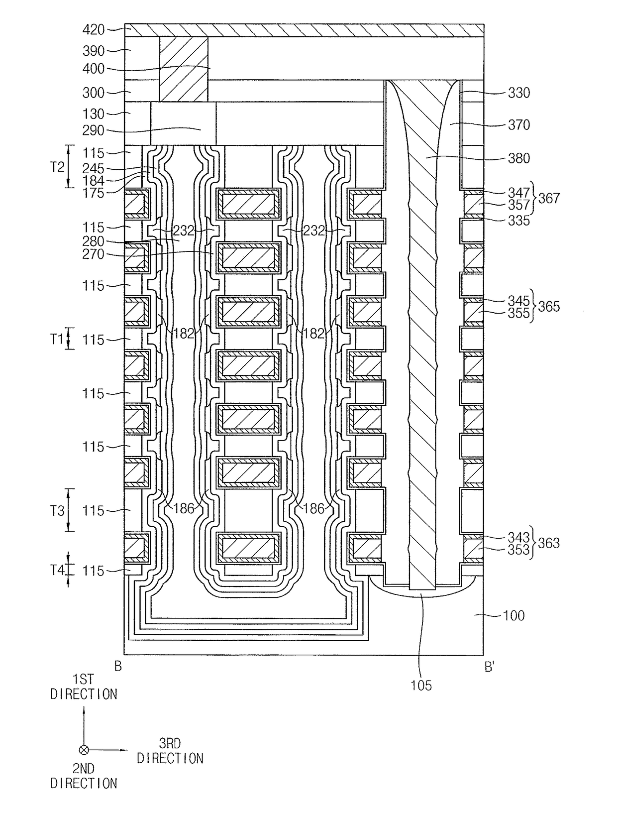
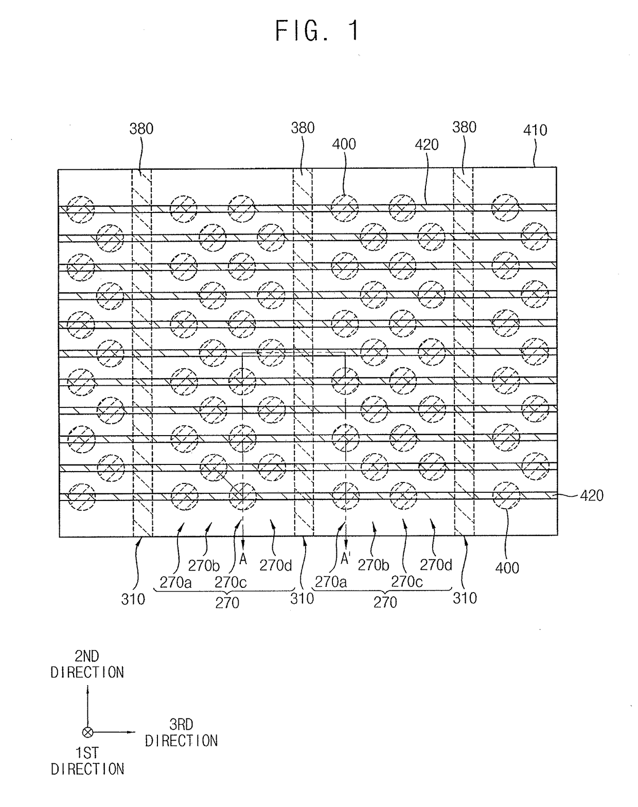
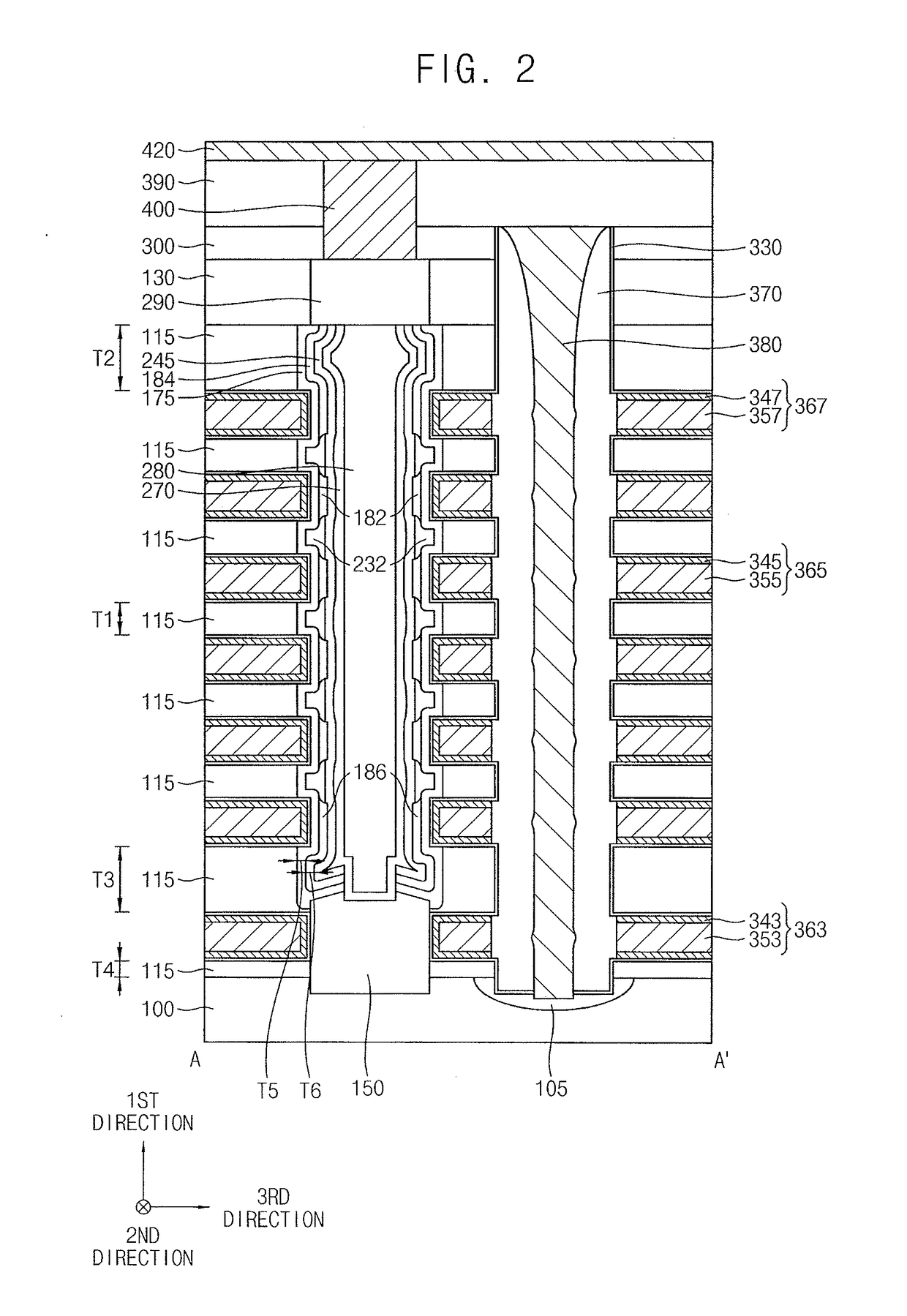
[0023]FIG. 1 illustrates an embodiment of a vertical memory device, and FIG. 2 illustrates a view taken along section line A-A′ in FIG. 1. For purposes of illustration, a direction substantially perpendicular to a top surface of a substrate is defined as a first direction, and two directions substantially parallel to the top surface of the substrate and crossing each other are defined as second and third directions, respectively. In example embodiments, the second and third directions may be substantially perpendicular to each other. Throughout the present disclosure, the first, second and third directions are as defined above and as shown in the drawings.

[0024]Referring to FIGS. 1 and 2, the vertical memory device may include a plurality of insulating interlayer patterns 115, a plurality of gate electrodes 363, 365 and 367, a channel 270, a charge storage pattern structure, and first filling patterns 232 on a substrate 100. The vertical memory device may further include a first sem...


PUM


Abstract

A vertical memory device includes insulating interlayer patterns, of gate electrodes, a channel, and a charge storage pattern structure. The insulating interlayer patterns are spaced in a first direction. The gate electrodes between are neighboring insulating interlayer patterns, respectively. The channel extends through the insulating interlayer patterns and the gate electrodes in the first direction. The charge storage pattern structure includes a tunnel insulation pattern, a charge trapping pattern structure, and a blocking pattern sequentially stacked between the channel and each of the gate electrodes in a second direction. The charge trapping pattern structure includes charge trapping patterns spaced in the first direction. The charge trapping patterns are adjacent to sidewalls of first gate electrodes, respectively. A first charge trapping pattern extends in the first direction along a sidewall of a first insulating interlayer pattern.

Description

CROSS-REFERENCE TO RELATED APPLICATION[0001]Korean Patent Application No. 10-2016-0010401, filed on Jan. 28, 2016, and entitled, “Vertical Memory Devices and Methods of Manufacturing the Same,” is incorporated by reference herein in its entirety.BACKGROUND[0002]1. Field[0003]One or more embodiments described herein relate to vertical memory devices and methods of manufacturing vertical memory devices.[0004]2. Description of the Related Art[0005]Producing highly integrated semiconductor devices continues to be a goal of designers. One way to increase integration is to increase the number of layers stacked in a vertical memory device, while at the same time reduce the thicknesses of those layers. However, reducing layer thickness may deteriorate the characteristics of the memory device, for example, due to coupling that may occur between neighboring, vertically arranged memory cells.SUMMARY[0006]In accordance with one or more embodiments, a vertical memory device includes a plurality ...

Claims


Application Information

Patent Timeline
Patent Type & Authority Applications(United States)
IPC IPC(8): H01L27/11582H01L29/792H01L29/423
CPCH01L27/11582H01L29/7926H01L29/42344H10B43/00H10B43/20H01L28/00H10B43/27
Inventor KANAMORI, KOHJIKANG, SHIN-HWANPARK, YOUNG-WOOPARK, JUNG-HOON
Owner SAMSUNG ELECTRONICS CO LTD
Why Eureka
Try Eureka