Operation scheme with charge balancing erase for charge trapping non-volatile memory
a non-volatile memory and operation scheme technology, applied in the direction of digital storage, instruments, transistors, etc., can solve the problems of poor charge retention, and large vt distribution of erase state, so as to improve endurance and reliability
- Summary
- Abstract
- Description
- Claims
- Application Information
AI Technical Summary
Benefits of technology
Problems solved by technology
Method used
Image
Examples
Embodiment Construction
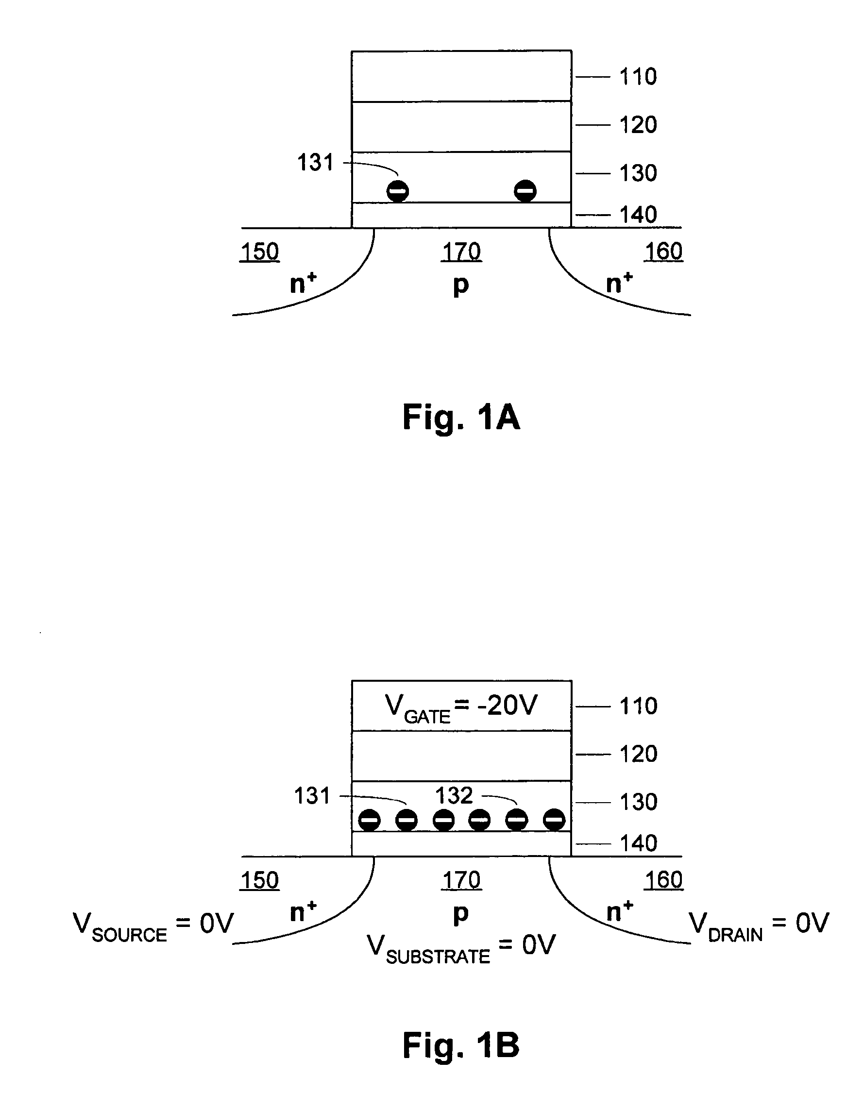
[0069]FIG. 1A is a simplified diagram of a charge trapping memory cell. The substrate includes n+ doped regions 150 and 160, and a p-doped region 170 between the n+ doped regions 150 and 160. The remainder of the memory cell includes a bottom dielectric structure 140 on the substrate, a charge trapping structure 130 on the bottom dielectric structure 140 (bottom oxide), a top dielectric structure 120 (top oxide) on the charge trapping structure 130, and a gate 110 on the oxide structure 120. Representative top dielectrics include silicon dioxide and silicon oxynitride having a thickness of about 5 to 10 nanometers, or other similar high dielectric constant materials including for example Al2O3. Representative bottom dielectrics include silicon dioxide and silicon oxynitride having a thickness of about 3 to 10 nanometers, or other similar high dielectric constant materials. Representative charge trapping structures include silicon nitride having a thickness of about 3 to 9 nanometers...
PUM
 Abstract
Description
Claims
Application Information


