Three-dimensional stacked and-type flash memory structure and methods of manufacturing and operating the same hydride

a flash memory structure and three-dimensional stacking technology, applied in the field of three-dimensional stacked and-type flash memory structure and manufacturing and operating the same, can solve the problems of time-consuming and expansive, and the expansive cost limit the staked layers of the 3d flash memory structure, and achieve the effect of improving read latency

Active Publication Date: 2013-04-30
MACRONIX INT CO LTD
View PDF2 Cites 138 Cited by
  • Summary
  • Abstract
  • Description
  • Claims
  • Application Information

AI Technical Summary

Benefits of technology

[0008]The disclosure relates to a 3D stacked AND-type flash memory structure and method of manufacturing the same are provided. The related operation methods such as reading, programming and erasing the 3D stacked AND-type flash memory structure of the embodiment are also described herein. The 3D stacked AND-type structure with improved read latency is suitable for a one-bit per cell operation and a two-bit per cell operation.

Problems solved by technology

However, the processes for manufacturing those three-dimensional NAND-type flash memory structures require several critical lithography steps for each memory layer, which is time-consuming and expansive.
Although the benefits of higher density are achieved using 3D arrays, the expansive costs limit the staked layers of the 3D flash memory structures.

Method used


Image

  • Three-dimensional stacked and-type flash memory structure and methods of manufacturing and operating the same hydride
  • Three-dimensional stacked and-type flash memory structure and methods of manufacturing and operating the same hydride
  • Three-dimensional stacked and-type flash memory structure and methods of manufacturing and operating the same hydride

Examples


Embodiment Construction

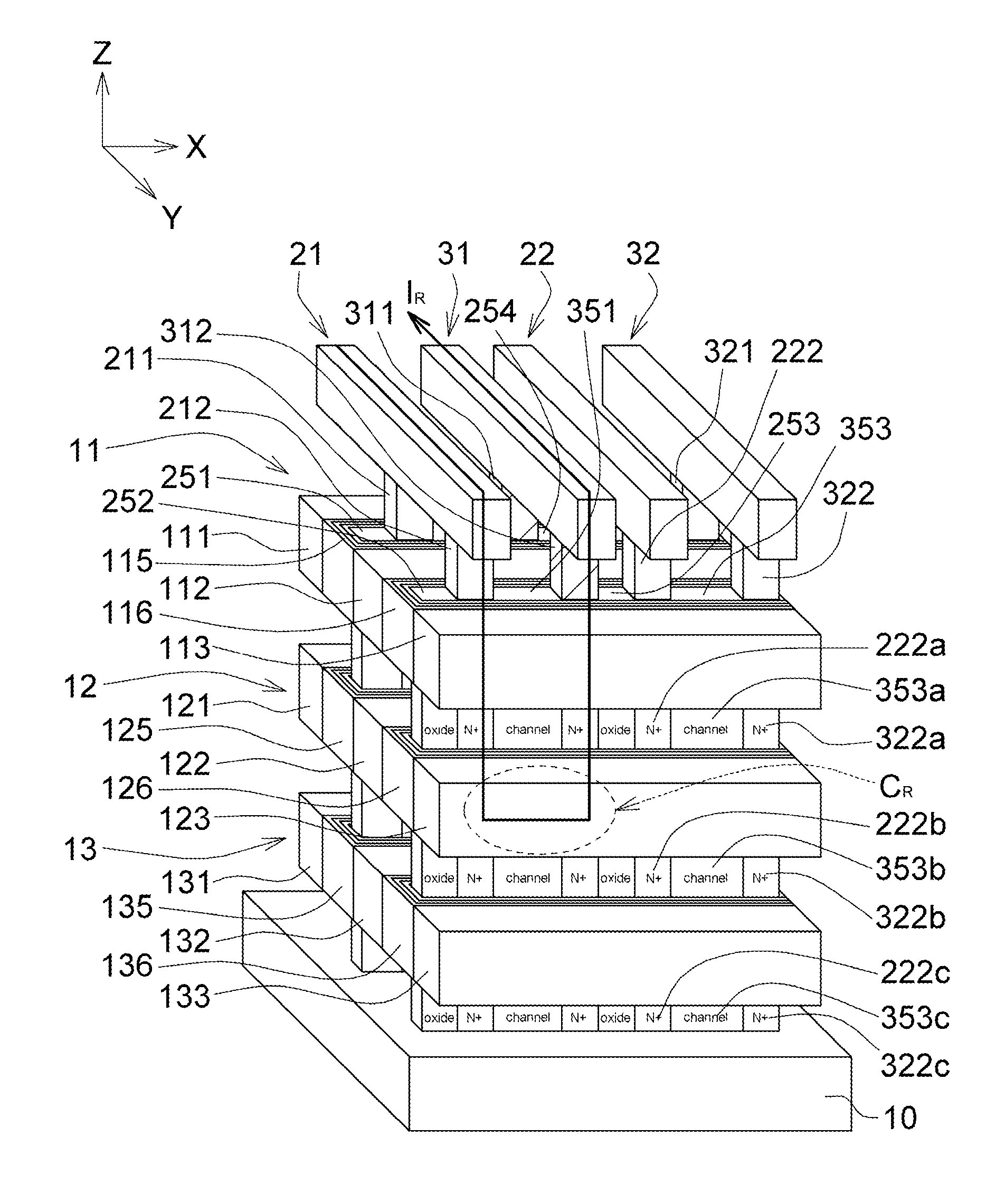
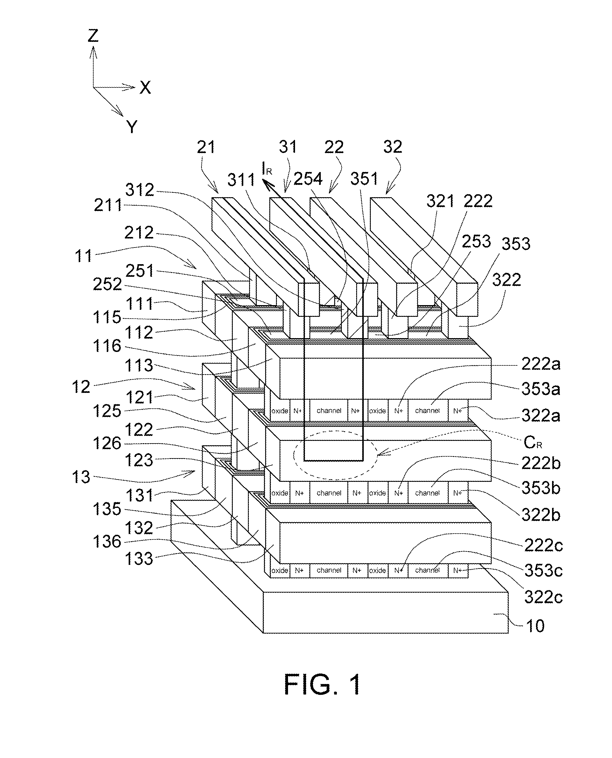
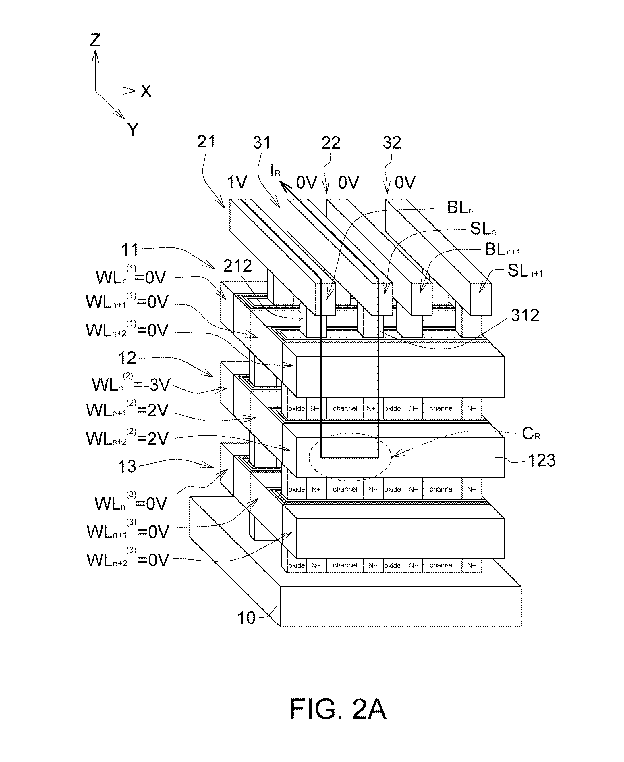
[0029]In the embodiment of the present disclosure, a 3D stacked AND-type flash memory structure and method of manufacturing the same are provided. Also, related operation methods such as reading, programming and erasing the 3D stacked AND-type flash memory structure of the embodiment are also described herein. The MOSFET (Metal-Oxide-Semiconductor Field-Effect Transistor) of the 3D stacked AND-type flash memory structure are connected in parallel instead of serially connected in the NAND-type flash memory structure; thus, the read latency can be greatly enhanced. Also, the 3D stacked AND-type flash memory structure of the embodiment can be programmed by channel hot electron programming (CHE) method like NOR Flash, or programmed by FN (Fowler-Nordheim) tunneling method like NAND Flash. In the embodiment of the present disclosure, the device is a double-gated charge-trapping device, and the double gates could be independently decoded, so that physically two bit / cell operation can be c...


PUM


Abstract

A 3D stacked AND-type flash memory structure comprises several horizontal planes of memory cells arranged in a three-dimensional array, and each horizontal plane comprising several word lines and several of charge trapping multilayers arranged alternately, and the adjacent word lines spaced apart from each other with each charge trapping multilayer interposed between; a plurality of sets of bit lines and source lines arranged alternately and disposed vertically to the horizontal planes; and a plurality of sets of channels and sets of insulation pillars arranged alternatively, and disposed perpendicularly to the horizontal planes, wherein one set of channels is sandwiched between the adjacent sets of bit lines and source lines.

Description

BACKGROUND[0001]1. Field of the Invention[0002]The disclosure relates in general to a three-dimensional (3D) flash memory structure and methods of manufacturing and operating the same, and more particularly to a 3D stacked AND-type flash memory structure and methods of manufacturing and operating the same.[0003]2. Description of the Related Art[0004]A nonvolatile semiconductor memory device is typically designed to securely hold data even when power is lost or removed from the memory device. Various types of nonvolatile memory devices have been proposed in the related art. Also, manufactures have been looking for new developments or techniques combination for stacking multiple planes of memory cells, so as to achieve greater storage capacity. For example, several types of multi-layer stackable thin-film transistor (TFT) NAND-type flash memory structures have been proposed.[0005]However, the processes for manufacturing those three-dimensional NAND-type flash memory structures require...

Claims


Application Information

Patent Timeline
Patent Type & Authority Patents(United States)
IPC IPC(8): G11C11/00
CPCH01L27/11524H01L27/11556G11C8/16G11C16/0416H10B41/35H10B41/27
Inventor LUE, HANG-TING
Owner MACRONIX INT CO LTD
Why Eureka
Try Eureka