Semiconductor sensor structures with reduced dislocation defect densities and related methods for the same

a sensor structure and sensor technology, applied in the field of semiconductor devices, can solve problems such as continuous demands

Active Publication Date: 2010-04-01
TAIWAN SEMICON MFG CO LTD
View PDF101 Cites 139 Cited by
  • Summary
  • Abstract
  • Description
  • Claims
  • Application Information

AI Technical Summary

Problems solved by technology

This drive has resulted in continual demands for integrating one type of semiconductor devices into another semiconductor process.

Method used


Image

  • Semiconductor sensor structures with reduced dislocation defect densities and related methods for the same
  • Semiconductor sensor structures with reduced dislocation defect densities and related methods for the same
  • Semiconductor sensor structures with reduced dislocation defect densities and related methods for the same

Examples


Embodiment Construction

[0029]Disclosed herein is a method of making semiconductor devices and semiconductor devices made thereof.

[0030]The method enables integration of non-silicon semiconductor devices into a silicon process such that silicon circuitry of the semiconductor device can be formed through standard silicon processes. This integration capability can be of great importance in using low band-width or high band-width semiconductor materials for making semiconductor device having p-n and p-i-n structures in silicon processes.

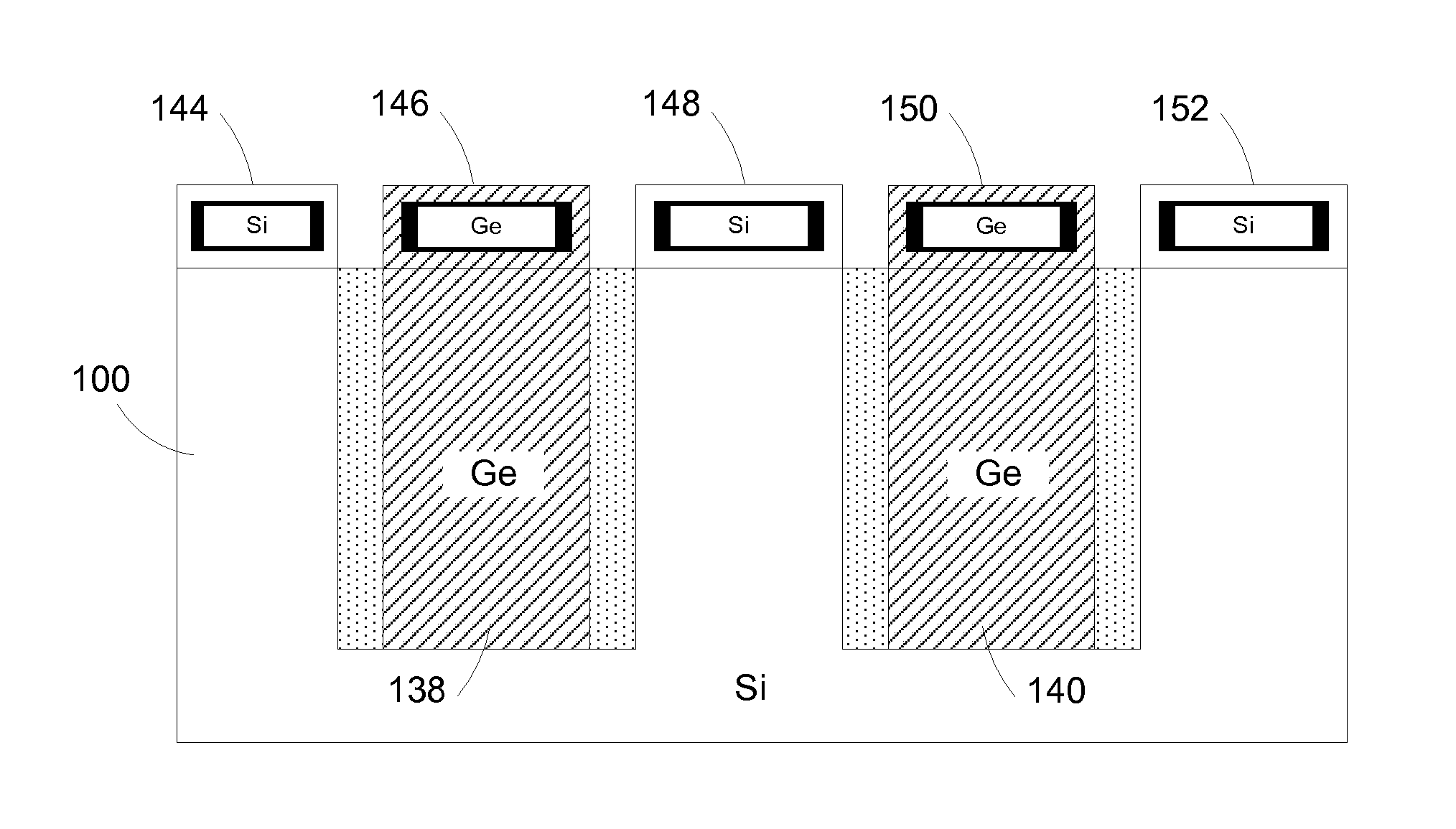
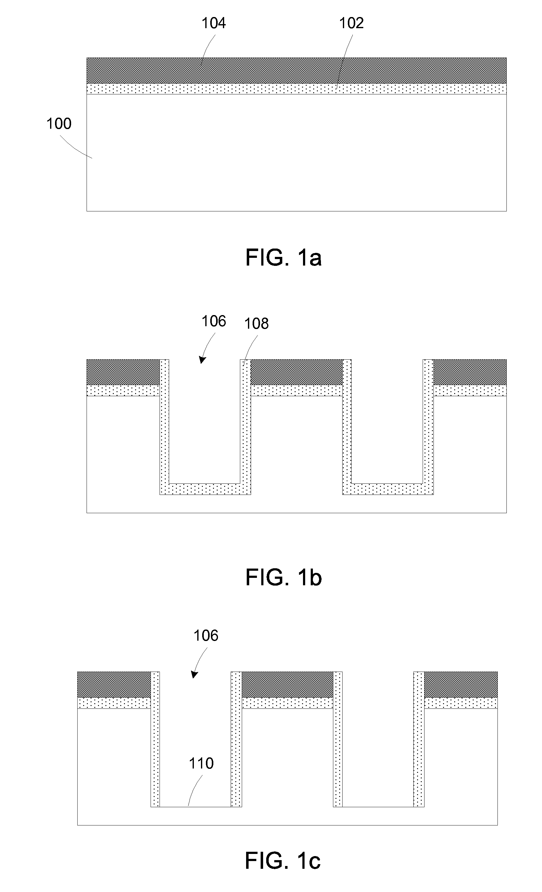
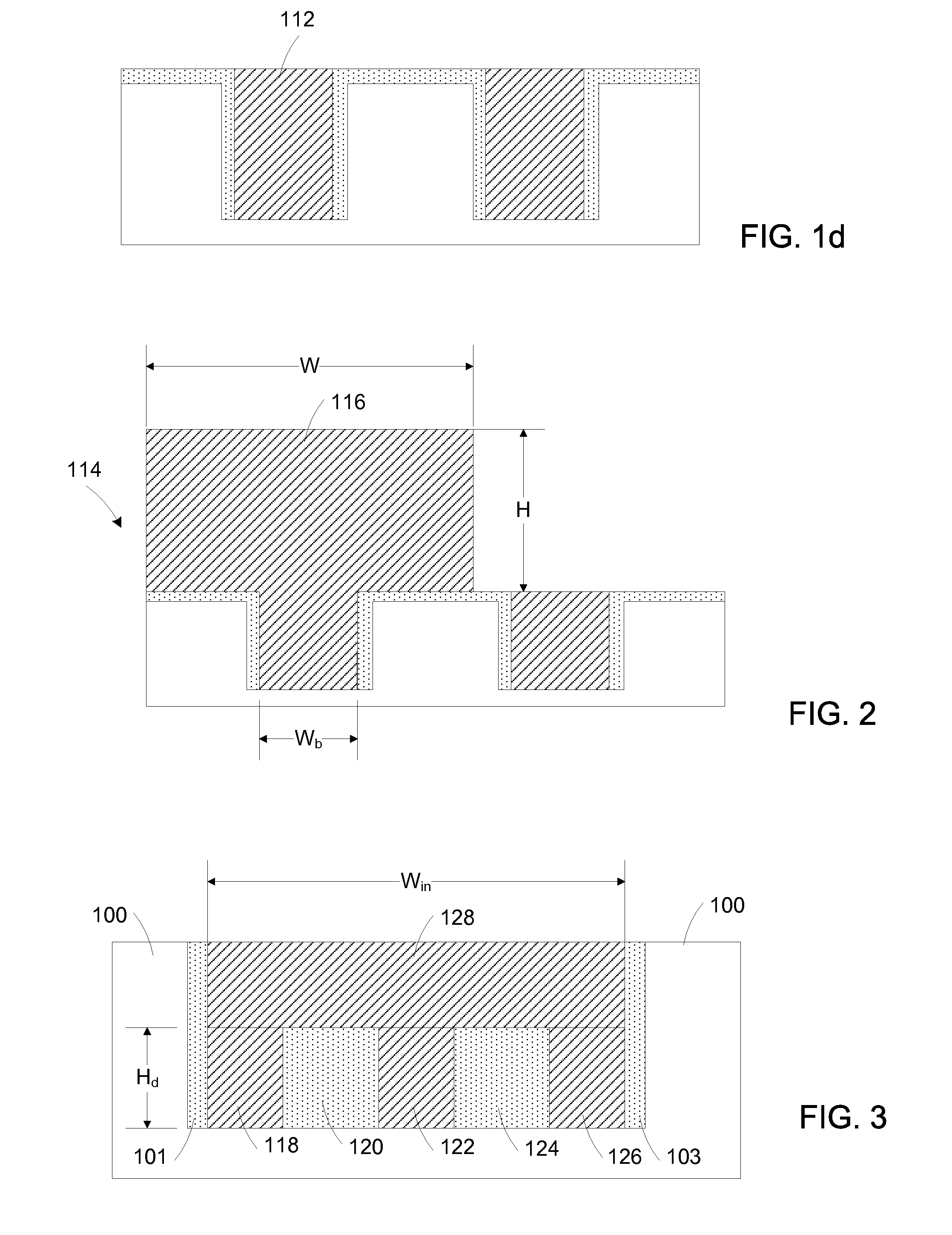
[0031]The method also enables forming ART (aspect-ratio-trapping) crystalline structures in a trench structure, such as a trench structure patterned by a trench patterning-process (e.g. a standard complementary-metal-oxide-semiconductor (CMOS) STI (shallow-trench-insulation) process) or a STI-like trench patterned structure. The semiconductor devices formed at or in the ART structure(s) can have any desired lateral and / or vertical dimensions that are substantially free from th...


PUM


Abstract

Non-silicon based semiconductor devices are integrated into silicon fabrication processes by using aspect-ratio-trapping materials. Non-silicon light-sensing devices in a least a portion of a crystalline material can output electrons generated by light absorption therein. Exemplary light-sensing devices can have relatively large micron dimensions. As an exemplary application, complementary-metal-oxide-semiconductor photodetectors are formed on a silicon substrate by incorporating an aspect-ratio-trapping technique.

Description

CROSS-REFERENCE TO RELATED APPLICATIONS[0001]The present application claims priority from U.S. provisional patent application, Ser. No. US 61 / 099,902, filed Sep. 24, 2008, entitled “Improved Semiconductor Sensor Structures with Reduced Dislocation Defect Densities and Related Methods for the Same” and is incorporated by reference herein and for which benefit of the priority dates is hereby claimed.TECHNICAL FIELD OF THE DISCLOSURE[0002]The technical field of this disclosure relates to the art of semiconductor devices; and more particularly to the art of methods of making semiconductor devices using aspect-ratio-trapping techniques and semiconductor devices made thereof.BACKGROUND OF THE DISCLOSURE[0003]There is a constant drive within the semiconductor industry to increase the performance and reduce the cost of semiconductor devices, such as photodetectors, diodes, light-emitting diodes, transistors, latches, and many other semiconductor devices. This drive has resulted in continual...

Claims


Application Information

Patent Timeline
Patent Type & Authority Applications(United States)
IPC IPC(8): H01L31/112H01L31/18H01L31/0248
CPCH01L21/02381H01L27/14643H01L21/02532H01L21/02639H01L21/02647H01L21/76224H01L27/1446H01L31/0304H01L31/03046H01L31/0312H01L31/103H01L31/1037H01L31/105Y02E10/544H01L21/02521Y02P70/50H01L27/14689H01L27/14612
Inventor CHENG, ZHIYUANFIORENZA, JAMES G.SHEEN, CALVINLOCHETEFELD, ANTHONY
Owner TAIWAN SEMICON MFG CO LTD
Why Eureka
Try Eureka