

Fabrication and structures of crystalline material
a technology of crystalline materials and fabrication, applied in the direction of basic electric elements, electrical equipment, semiconductor devices, etc., to achieve the effect of reducing surface roughness, reducing surface roughness, and reducing surface roughness
- Summary
- Abstract
- Description
- Claims
- Application Information
AI Technical Summary
Benefits of technology
Problems solved by technology
Method used
Image

Examples
Embodiment Construction
[0033]Reference will now be made in detail to the embodiments of the present general inventive concept, examples of which are illustrated in the accompanying drawings, wherein like reference numerals refer to like elements throughout. The embodiments are described below in order to explain the present general inventive concept by referring to the figures.
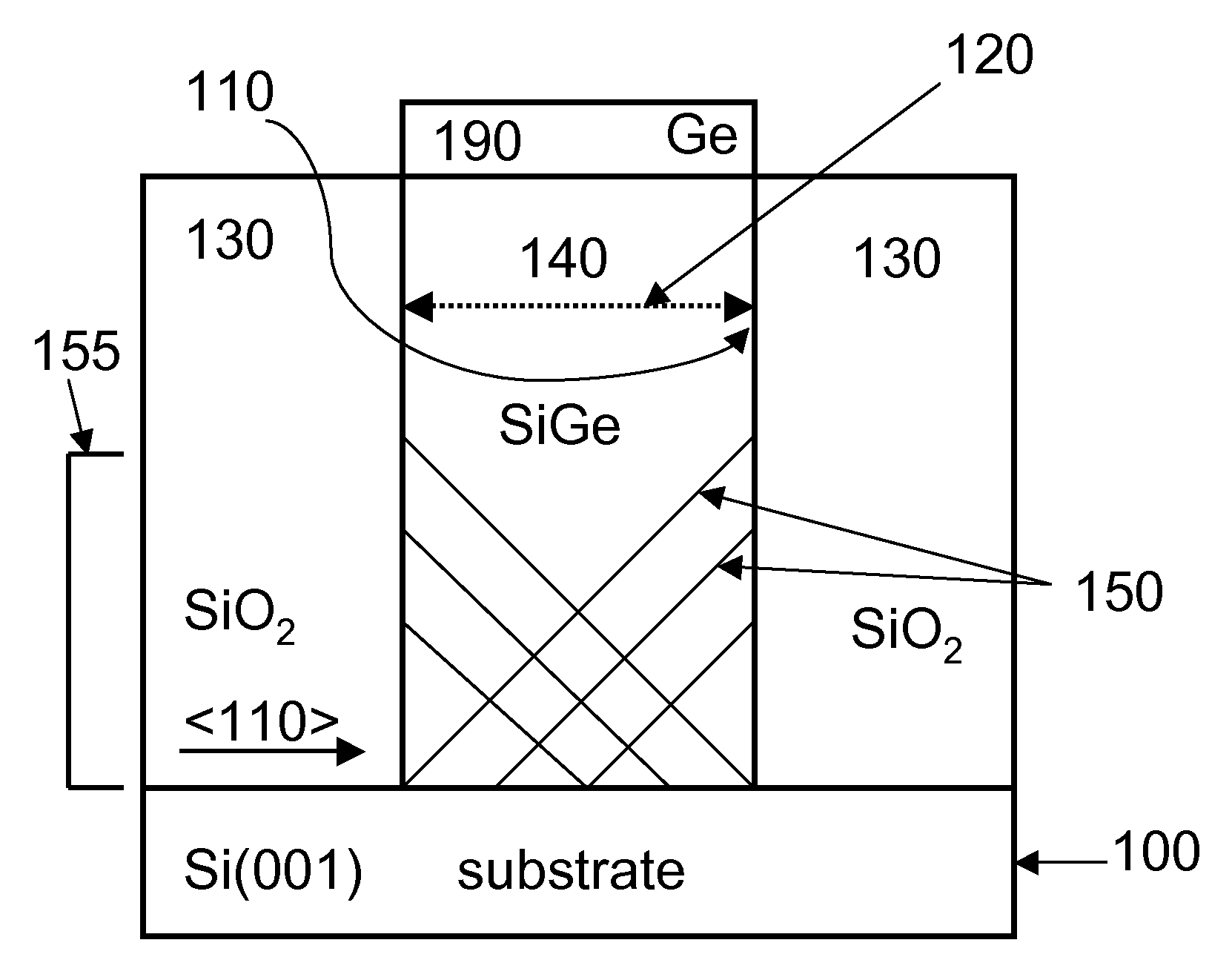
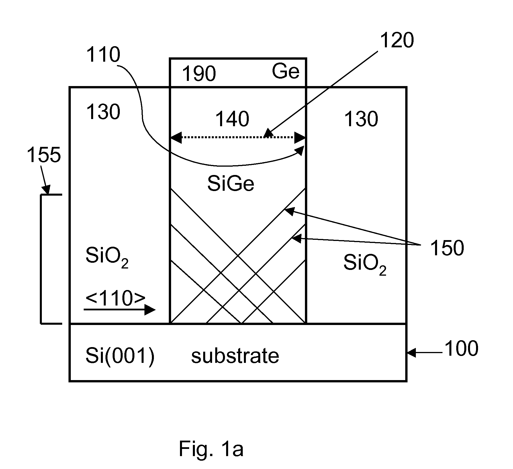
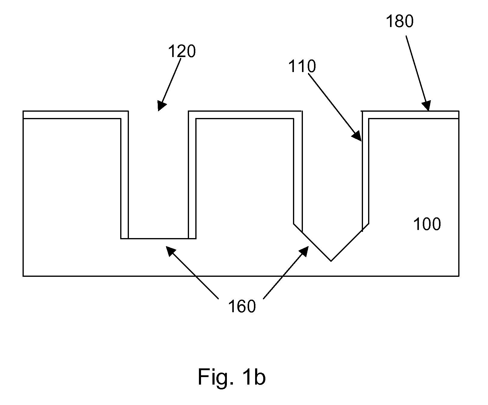
[0034]The formation of lattice-mismatched materials has many practical applications. For example, heteroepitaxial growth of group IV materials or compounds, and III-V, III-N and II-VI compounds on a crystalline substrate, such as silicon, has many applications such as photovoltaics, resonant tunneling diodes (RTD's), transistors (e.g., FET (which can be planar or 3D (e.g., finFET), HEMT, etc.), light-emitting diodes and laser diodes. As one example, heteroepitaxy of germanium on silicon is considered a promising path for high performance p-channel metal-oxide-semiconductor (MOS) field-effect transistors (FET) and for integrating opt...
PUM
 Abstract
Description
Claims
Application Information