

Drive unit
a technology of drive signal and drive signal, which is applied in the direction of electronic switching, pulse technique, semiconductor devices, etc., can solve the problems of increasing the electric power consumption of the first transistor, affecting the response time, and taking a substantial time from receiving the trigger of the drive signal, so as to achieve the effect of shortening the response tim
- Summary
- Abstract
- Description
- Claims
- Application Information
AI Technical Summary
Benefits of technology
Problems solved by technology
Method used
Image

Examples
first embodiment
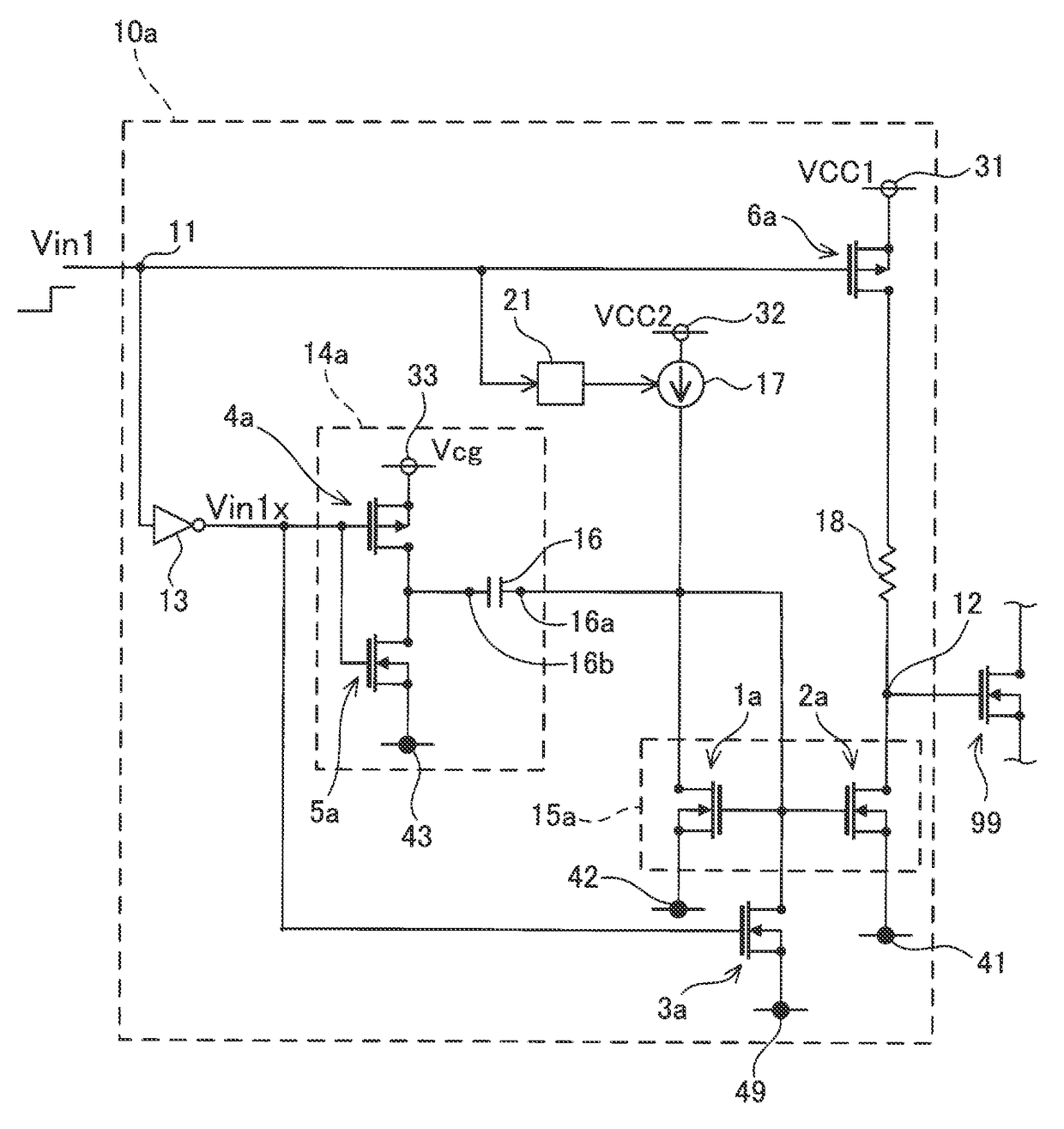
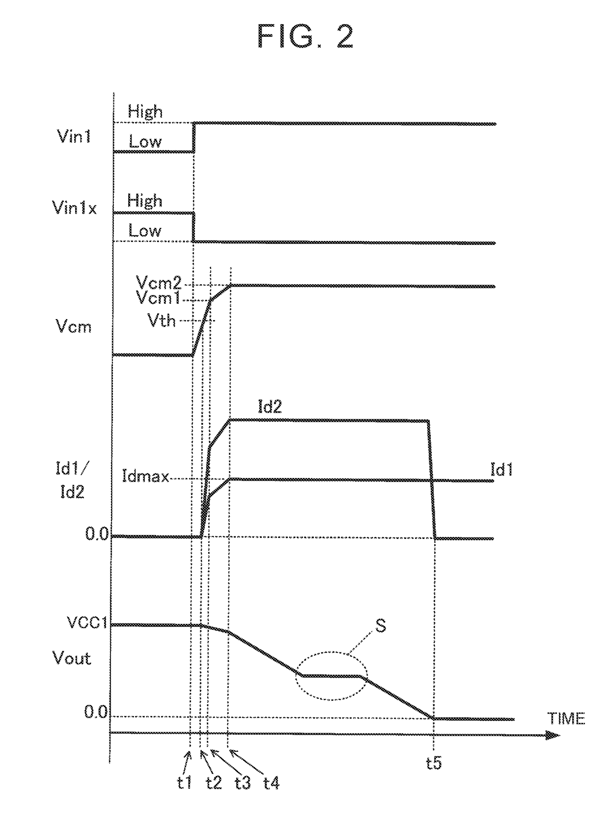
[0055]Referring to FIG. 1 and FIG. 2, a drive unit of a first embodiment will be described. FIG. 1 is a block diagram of the drive unit 10a. FIG. 2 is a time chart showing operation of the drive unit 10a. The drive unit 10a is a unit or system for driving a power transistor 99. The power transistor 99 is a switching device used for converting electric power. For example, the power transistor 99 is a switching device of an inverter that converts direct current into alternating current, or a switching device of a voltage converter. A power conversion system including the power transistor 99 is not illustrated in the drawings, except for the power transistor 99. When the power conversion system includes two or more power transistors, the drive unit 10a is prepared for each of the power transistors.
[0056]The drive unit 10a switches the power transistor 99 between ON and OFF, based on a pulsed drive signal Vin1 received from a high-order control unit (not shown). The drive unit 10a drive...
second embodiment
[0094]Referring to FIG. 4, a second embodiment will be described. In the drive unit 10a of the first embodiment, the sixth transistor 6a is connected between the power-supply positive terminal 31 and the output terminal 12, and the second transistor 2a of the current mirror circuit 15a is connected between the output terminal 12 and the power-supply negative terminal 41. On the other hand, in a drive unit 10b of the second embodiment, the second transistor 2 of the current mirror circuit 15a is connected between the power-supply positive terminal 31 and the output terminal 12, and the resistor 18 and a sixth transistor 106a are connected between the output terminal 12 and the power-supply negative terminal 41. A gate of the sixth transistor 106a is connected to the NOT device 13, and the inversion signal Vin1x is transmitted to the gate of the sixth transistor 106a. The power-supply negative terminal 42 is controlled so as to be at the same voltage as the output terminal 12.
[0095]In...
third embodiment
[0098]Referring to FIG. 5, a drive unit 10c of a third embodiment will be described. In the drive unit 10c of the third embodiment, a gate charge circuit 14b is different from the gate charge circuit 14a of the drive unit 10a of the first embodiment. In the block diagram of FIG. 5, the devices other than the gate charge circuit 14b are identical with the corresponding devices shown in the block diagram of FIG. 1, and therefore, will not be described.
[0099]Like the gate charge circuit 14a of the first embodiment, the gate charge circuit 14b is connected to the drain and gate of the first transistor 1a, and the gate of the second transistor 2a. The gate charge circuit 14b consists of the power-supply positive terminal 33 to which the voltage Vcg is supplied, a voltage-driven type P-channel fourth transistor 104a, and a diode 19. A cathode 19a of the diode 19 is connected to the drain and gate of the first transistor 1a, and the gate of the second transistor 2a. An anode 19b of the dio...
PUM
 Abstract
Description
Claims
Application Information