
Control interface device and fingerprint sensor

a technology of which is applied in the field of control interface device and fingerprint sensor, can solve the problems of sensitivity and dynamic problems of detection electronics, degrade measurement, and require a more complex management to reconstitute fingerprint imag

Active Publication Date: 2017-10-05
QUICKSTEP TECH
View PDF16 Cites 3 Cited by
  • Summary
  • Abstract
  • Description
  • Claims
  • Application Information

AI Technical Summary

Benefits of technology

The patent text describes a technology that prevents unwanted electrical effects in a device by using special surfaces called guards. These guards are placed close to the device's electrodes and are charged to the same electric potential as the electrodes. This prevents the formation of unwanted capacitances between the guards and the electrodes. The guards have openings that allow measurements to be taken and cover the areas around the electrodes to avoid interference with object detection. The technology prevents issues that can affect the accuracy of the device's measurements and improves overall performance.

Problems solved by technology

In terms of integration cost, the linear sensors are more economical, but they require a more complex management to reconstitute the image of the fingerprint.
This causes sensitivity and dynamic problems for the detection electronics.
Also, in so far as all the electrodes are implemented in the same layer of the touchpad under the protective glass, the fingerprint sensor electrodes are too far away from the finger, which additionally generates sensitivity problems and a phenomenon of spatial skewing or averaging of the relief of the fingerprints which degrades the measurement.

Method used


Image

  • Control interface device and fingerprint sensor
  • Control interface device and fingerprint sensor
  • Control interface device and fingerprint sensor

Examples


second embodiment

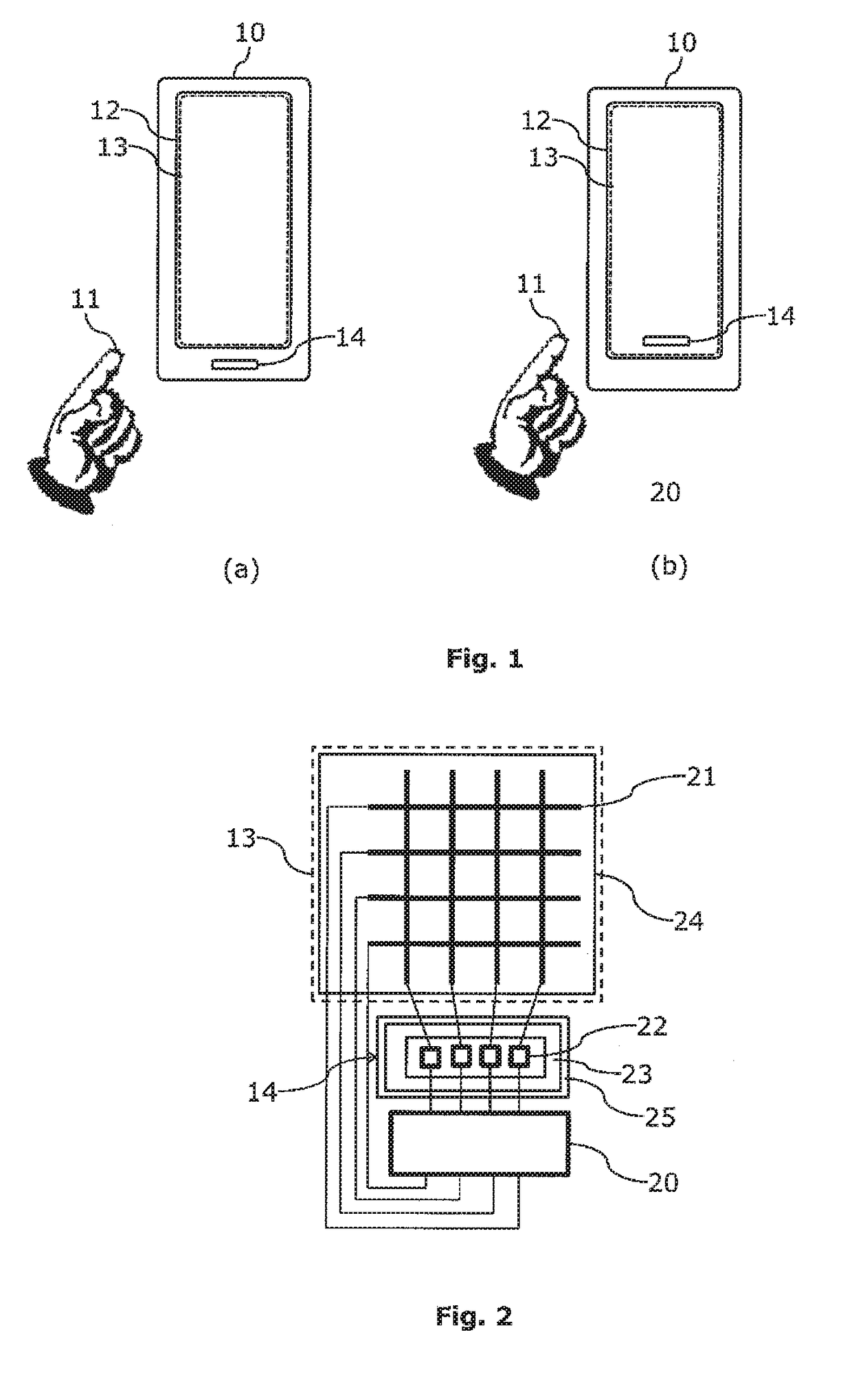
[0066]FIG. 1(a) and FIG. 1(b) show respectively a first and second embodiment of the apparatus according to the invention.

[0067]FIG. 2 shows a first embodiment of the interface device according to the invention.

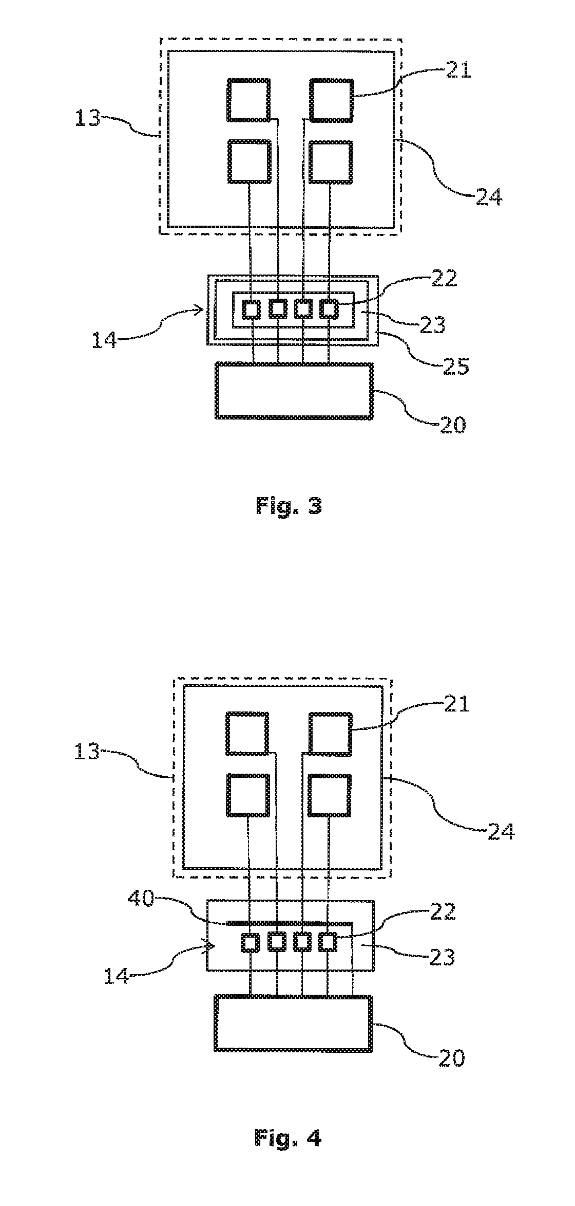
[0068]FIG. 3 shows a second embodiment of the interface device according to the invention.

[0069]FIG. 4 shows a third embodiment of the interface device according to the invention.

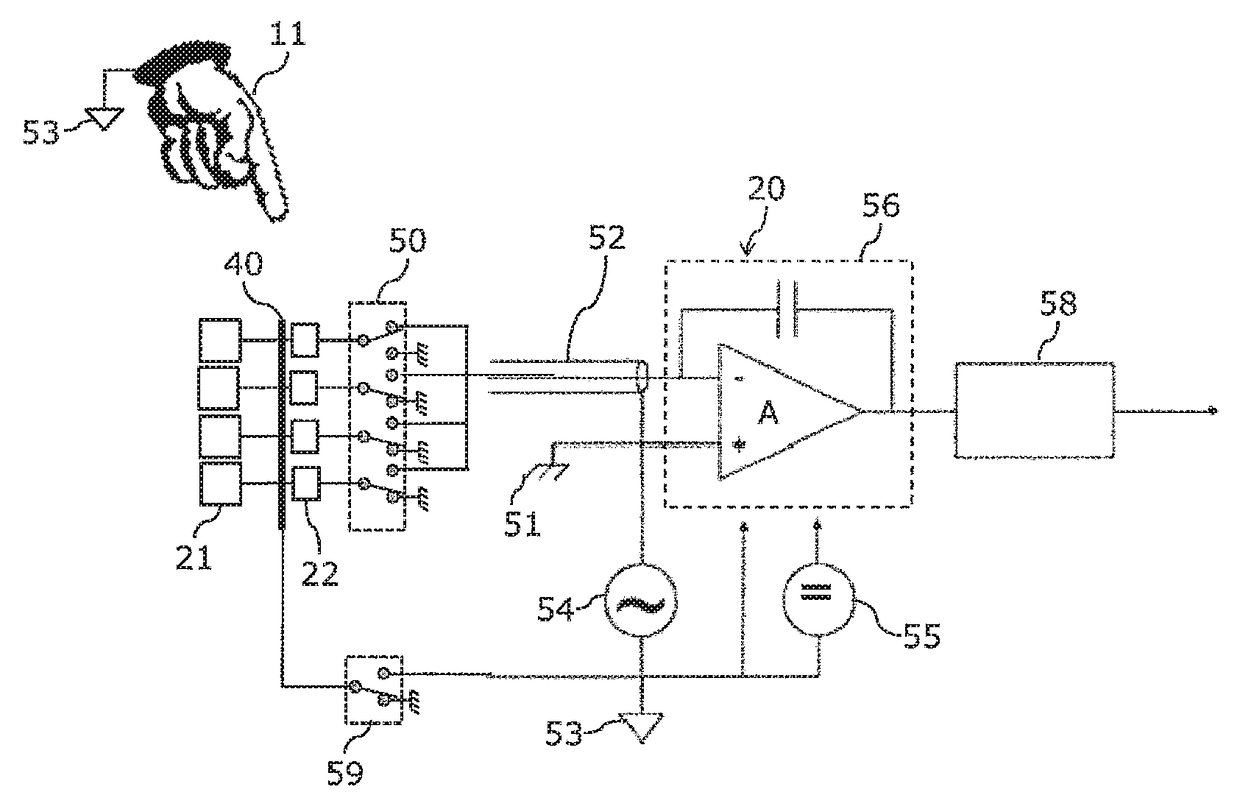
[0070]FIG. 5 shows an embodiment of detection electronics according to the invention.

[0071]It is well understood that the embodiments which will be described in the following are in no way limiting. One could in particular imagine variants of the invention only comprising a selection of features subsequently described isolated from other features described, if this selection of features is sufficient to confer a technical advantage or for distinguishing the invention from the state of the prior art. This selection includes at least one preferably functional feature without structural details, or with...


PUM


Abstract

The present invention relates to a device or apparatus comprising a touch surface provided with first capacitive measurement electrodes (21), a fingerprint sensor (14) provided with second capacitive measurement electrodes (22) distinct from the first electrodes (21), capacitive electronic detection means (20) arranged so as to allow the detection of control objects (11) in a neighborhood of the first electrodes (21) by measuring a capacitive coupling between said first measurement electrodes (21) and said control objects (11) wherein said capacitive electronic detection means (20) comprise inputs electrically connected simultaneously to at least one first measurement electrode (21) and at least one second measurement electrode (22).

Description

TECHNICAL DOMAIN[0001]This invention relates to a tactile interface and fingerprint reader device. It also relates to an apparatus comprising such a device.[0002]The domain of the invention is more specifically, but without limitation, that of human-machine interface devices.STATE OF THE PRIOR ART[0003]More and more portable apparatuses, in particular of smart phone or tablet type, are equipped with a security device using a fingerprint reader.[0004]This fingerprint reader is used in order to identify the user, for example to authorize unlocking the apparatus or execution of another function.[0005]The most widespread technologies for implementing fingerprint readers use capacitive measurement. These technologies have the advantage of being discreet, non-bulky, and energy-efficient and provide a good level of reliability.[0006]There are two main families of capacitive sensors used for reading fingerprints:[0007]Matrix sensors or called “total pixel matrix sensors” which comprise a ma...

Claims


Application Information

Patent Timeline
IPC IPC(8): G06F3/041G06K9/00G06F3/044
CPCG06F3/0418G06F2203/04107G06K9/0002G06F3/044G06F3/0443G06F3/04164G06V40/1306
Inventor ROZIERE, DIDIER
Owner QUICKSTEP TECH
Learn More