Supercharge Your Innovation With Domain-Expert AI Agents!

Impedance calibration circuit and semiconductor memory apparatus having the same

Active Publication Date: 2017-10-19
SK HYNIX INC
View PDF2 Cites 0 Cited by
  • Summary
  • Abstract
  • Description
  • Claims
  • Application Information

AI Technical Summary

Benefits of technology

The patent describes an impedance calibration circuit and a semiconductor memory apparatus that includes it. The circuit includes a first reference resistor and a second reference resistor that is connected to the first resistor in parallel. The second reference resistor's resistance value changes depending on the operation voltage mode. The circuit also includes a calibration circuit that generates a calibration code based on the resistance values of the first and second reference resistors. The calibration code is used to calibrate an impedance value in the semiconductor memory apparatus's calibration pad. Additionally, the apparatus also includes a data input / output driver that calibrates an impedance value of an output signal based on the calibration code. The technical effects of this patent include improved accuracy in impedance calibration and more efficient calibration of semiconductor memory apparatuses.

Problems solved by technology

As the swing width of the signal is reduced, the effect on external noise may be increased, and impedance mismatching of an interface of the semiconductor memory apparatus may occur.
The impedance mismatching may be caused by the external noise, change in a power voltage, variation of an operation temperature, and change in a fabrication process.

Method used


Image

  • Impedance calibration circuit and semiconductor memory apparatus having the same
  • Impedance calibration circuit and semiconductor memory apparatus having the same
  • Impedance calibration circuit and semiconductor memory apparatus having the same

Examples


Embodiment Construction

”.

BRIEF DESCRIPTION OF THE DRAWINGS

[0012]The above and other aspects, features and advantages of the subject matter of the present disclosure will be more clearly understood from the following detailed description taken in conjunction with the accompanying drawings, in which:

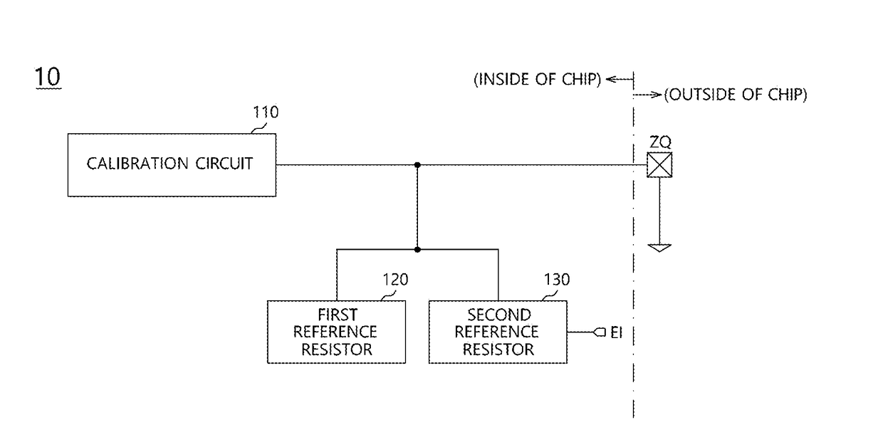
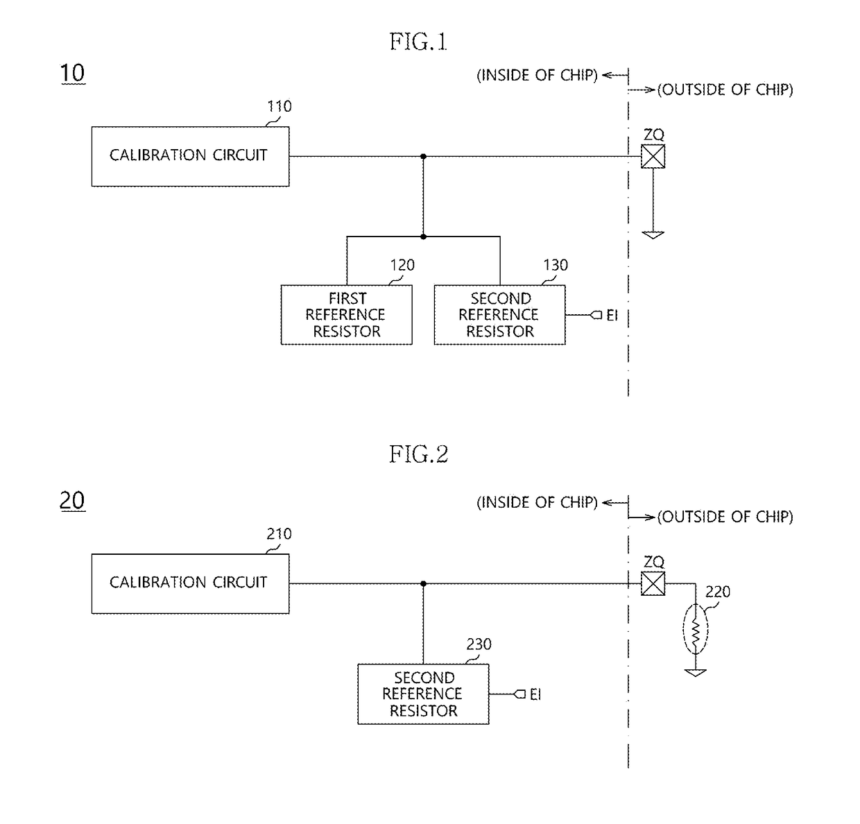
[0013]FIG. 1 is a configuration diagram illustrating an impedance calibration circuit according to an embodiment of the disclosure;

[0014]FIG. 2 is a configuration diagram illustrating an impedance calibration circuit according to an embodiment of the disclosure;

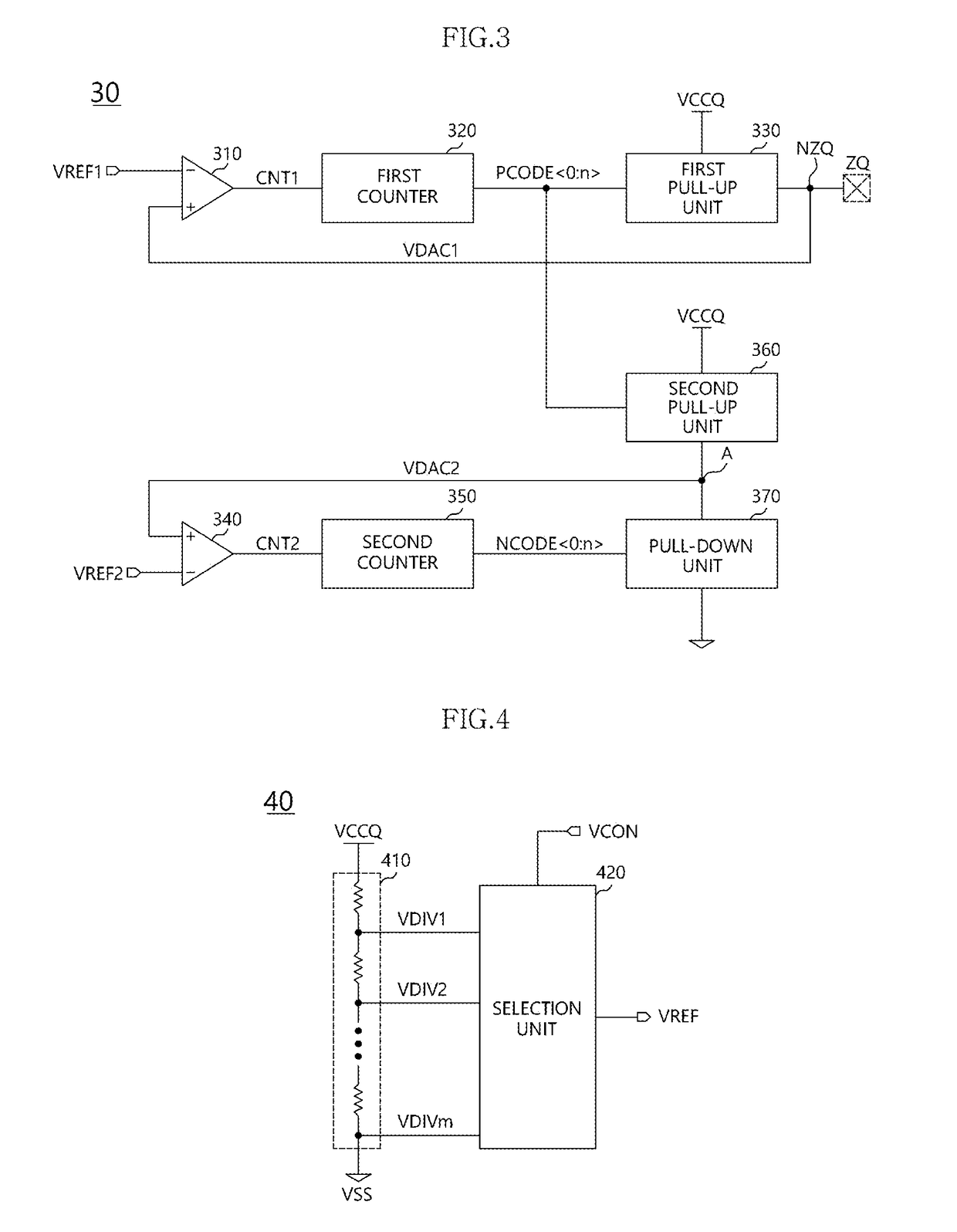
[0015]FIG. 3 is a configuration diagram illustrating a calibration circuit according to an embodiment of the disclosure;

[0016]FIG. 4 is a configuration diagram illustrating a reference voltage generation circuit according to an embodiment of the disclosure;

[0017]FIG. 5 is a configuration diagram illustrating a pull-up unit according to an embodiment of the disclosure;

[0018]FIG. 6 is a configuration diagram illustrating a semiconductor memory apparatus acc...


PUM


Abstract

An impedance calibration circuit includes a first reference resistor electrically coupled to a calibration pad, a second reference resistor which is coupled to the first reference resistor in parallel and a resistance value of the second reference resistor is varied according to an operation voltage mode, and a calibration circuit electrically coupled to the calibration pad and configured to generate a calibration code according to a resistance value formed by the first reference resistor and the second reference resistor and calibrate an impedance value in the calibration pad according to the calibration code.

Description

CROSS-REFERENCES TO RELATED APPLICATION[0001]This application claims priority under 35 U.S.C. 119(a) to Korean application No. 10-2016-0045599, filed on Apr. 14, 2016, in the Korean intellectual property Office, which is incorporated by reference in its entirety as set forth in full.BACKGROUND1. Technical Field[0002]Various embodiments of the inventive concept relate to a semiconductor integrated apparatus, and more particularly, to an impedance calibration circuit and a semiconductor memory apparatus having the same.2. Related Art[0003]Semiconductor memory apparatuses may include a receiving circuit configured to receive a signal transmitted from an external apparatus and a transmitting circuit configured to transmit an internal signal to the external apparatus.[0004]Swing widths of signals received and transmitted in and from the receiving circuit and the transmitting circuit of the semiconductor memory apparatus are relevant to speed of the semiconductor memory apparatus. That is...

Claims


Application Information

Patent Timeline
IPC IPC(8): H03K19/00G11C7/10G11C7/12G11C7/22
CPCH03K19/0005G11C7/22G11C7/10G11C7/12G11C7/1057G11C29/022G11C29/025G11C29/028G11C2207/2254G11C7/1084G11C7/04
Inventor JANG, DONG WOOK
Owner SK HYNIX INC
Features
  • R&D
  • Intellectual Property
  • Life Sciences
  • Materials
  • Tech Scout
  • Unparalleled Data Quality
  • Higher Quality Content
  • 60% Fewer Hallucinations
Learn More