Photoconductor, image forming apparatus, and process cartridge

Active Publication Date: 2017-10-26
RICOH KK
View PDF2 Cites 4 Cited by
  • Summary
  • Abstract
  • Description
  • Claims
  • Application Information

AI Technical Summary

Problems solved by technology

As a result, the photoconductor is deteriorated in electrical properties, and cannot retain electric stability when the photoconductor is used over a long period.
Particularly, a titanyl photocyanine pigment used as a charge-generating material in a charge-generating layer has excellent sensitivity properties against light in a region of from a long-wavelength range to a short-wavelength range, but has a problem that generated photo car

Method used


Image

  • Photoconductor, image forming apparatus, and process cartridge
  • Photoconductor, image forming apparatus, and process cartridge
  • Photoconductor, image forming apparatus, and process cartridge

Examples


first embodiment

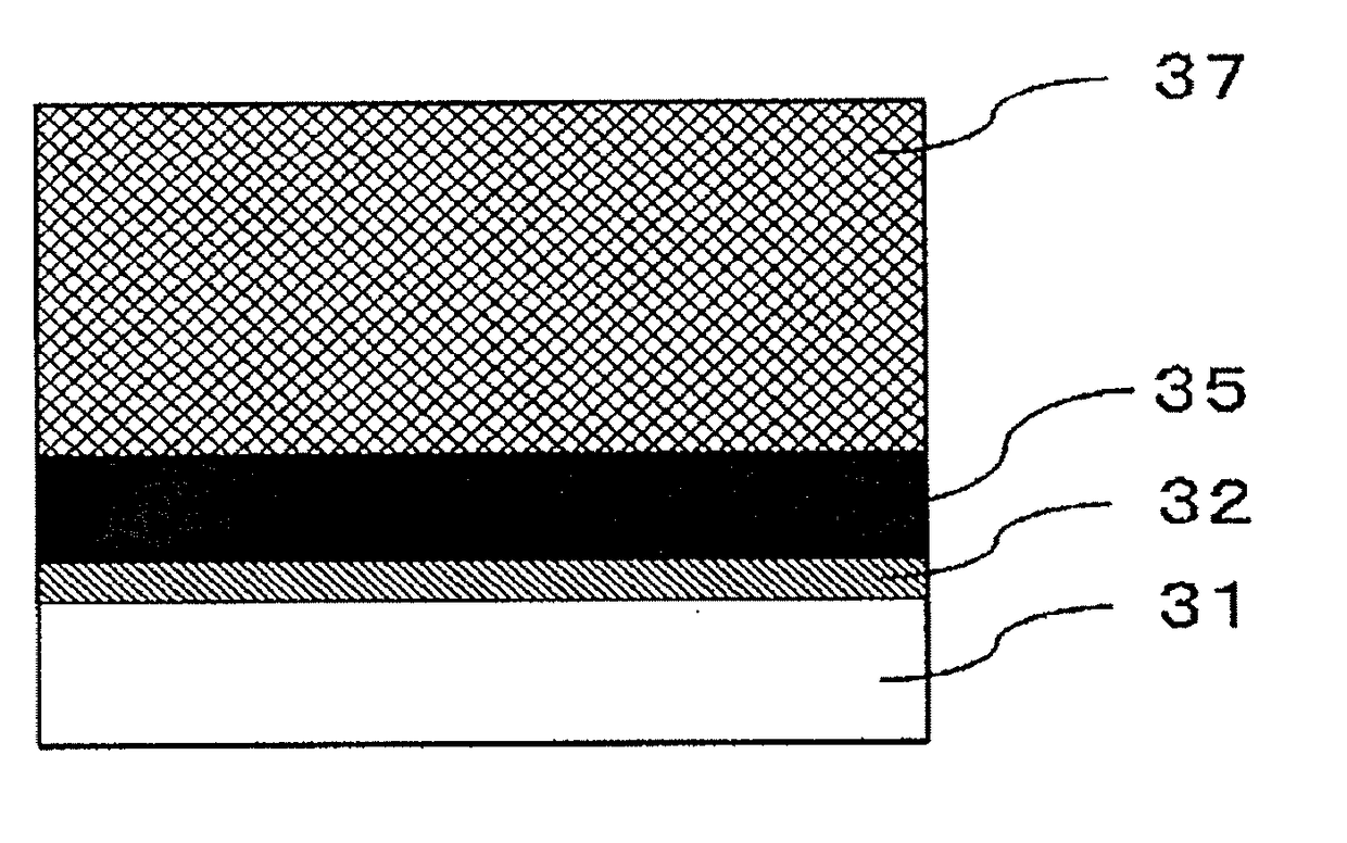
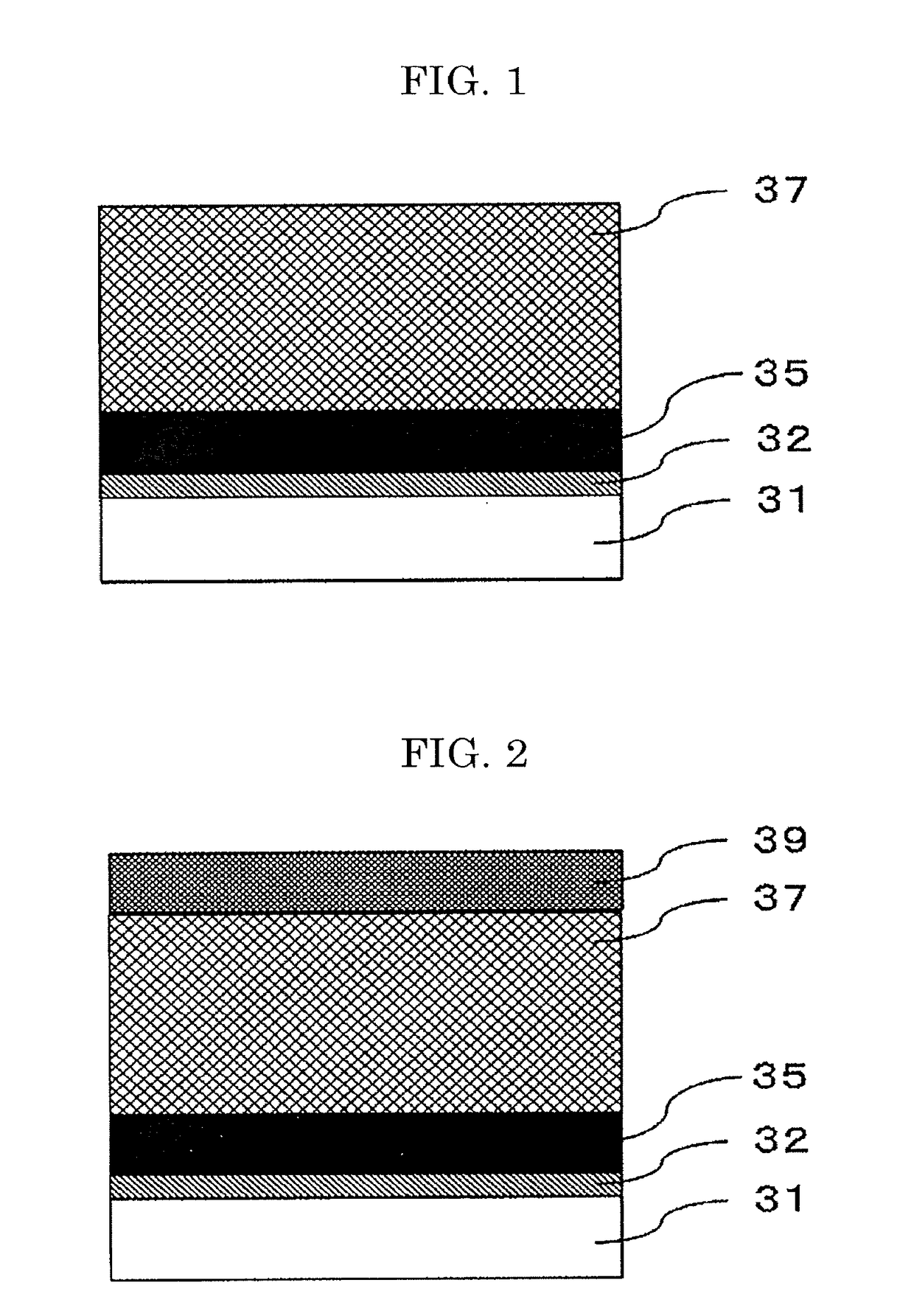
[0135]A layer configuration of the photoconductor according to a first embodiment will be described with reference to FIG. 1.

[0136]FIG. 1 illustrates a structure including a laminate photoconductive layer, and illustrates a layer configuration of the photoconductor where an undercoat layer 32, a charge-generating layer 35, and a charge-transporting layer 37 are sequentially disposed on a conductive support 31. Note that, a combination of the charge-generating layer 35 and the charge-transporting layer 37 corresponds to a photoconductive layer.

second embodiment

[0137]A layer configuration of the photoconductor according to a second embodiment will be described with reference to FIG. 2.

[0138]FIG. 2 illustrates a structure including a laminate photoconductive layer, and illustrates a layer configuration of the photoconductor where an undercoat layer 32, a charge-generating layer 35, a charge-transporting layer 37, and a protective layer 39 are sequentially disposed on a conductive support 31. Note that, a combination of the charge-generating layer 35 and the charge-transporting layer 37 corresponds to a photoconductive layer.

(Image Forming Apparatus)

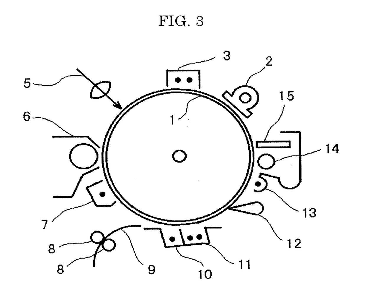
[0139]An image forming apparatus of the present disclosure includes at least a photoconductor, a charging unit configured to charge a surface of the photoconductor, an exposing unit configured to expose the surface charged of the photoconductor to light to form an electrostatic latent image, a developing unit configured to develop the electrostatic latent image with a toner to form a visible imag...

example 1

[0185]After applying Undercoat-Layer Coating Liquid A-1 onto an aluminium cylinder (diameter: 100 mm, length: 380 mm) through dip coating, the applied coating liquid was dried for 30 minutes at 170° C., to form an undercoat layer having an average film thickness of 5 μm disposed on the aluminium cylinder. Next, Charge-Generating-Layer Coating Liquid B-1 was applied by dip coating followed by drying for 30 minutes at 90° C., to form a charge-generating layer having an average film thickness of 0.2 μm disposed on the undercoat layer. Moreover, Charge-Transporting-Layer Coating Liquid C was applied by dip coating, followed by performing drying for 30 minutes at 150° C., to thereby form a charge-transporting layer having an average film thickness of 25 μm disposed on the charge-generating layer. In the manner as described, Photoconductor 1 of Example 1 was produced.


PUM

PropertyMeasurementUnit
Thicknessaaaaaaaaaa
Thicknessaaaaaaaaaa
Thicknessaaaaaaaaaa

Abstract

A photoconductor including a conductive support, an undercoat layer, a charge-generating layer, and a charge-transporting layer, at least the undercoat layer, the charge-generating layer, and the charge-transporting layer being disposed on the conductive support in an order mentioned, wherein the undercoat layer includes a binder resin and metal oxide particles, and the charge-generating layer includes a binder resin, a titanyl phthalocyanine pigment, and a salicylic acid derivative.

Description

CROSS-REFERENCE TO RELATED APPLICATIONS[0001]The present application claims priority under 35 U.S.C. §119 to Japanese Patent Application No. 2016-087269, filed Apr. 25, 2016. The contents of which are incorporated herein by reference in their entirety.BACKGROUND OF THE INVENTIONField of the Invention[0002]The present disclosure relates to a photoconductor, an image forming apparatus including the photoconductor, and a process cartridge including the photoconductor.Description of the Related Art[0003]In an image forming method using an image forming apparatus, an image is formed by performed steps, such as a charging step, an exposing step, a developing step, and transferring step on a photoconductor (also referred to as an electrophotographic photoconductor, an electrostatic-latent-image-bearing member, or an image bearer). Recently, an organic photoconductor including an organic material is widely used as a photoconductor because of advantages, such as flexibility, thermal stabilit...

Claims


Application Information

Patent Timeline
IPC IPC(8): G03G5/047G03G5/14G03G5/10G03G5/06G03G5/05G03G15/00
CPCG03G5/047G03G15/75G03G5/0696G03G5/0542G03G5/144G03G5/0614G03G5/0564G03G5/0525G03G5/102G03G5/0517G03G5/142G03G5/06147G03G5/0612
Inventor ASANO, TOMOHARUSUZUKI, TETSUROKURIMOTO, EIJINII, DAISUKEISHIDA, TOSHIHIRO
Owner RICOH KK
Why Eureka
Try Eureka