Edge termination designs for super junction device

Active Publication Date: 2017-11-23
HUNTECK SEMICON (SHANGHAI) LTD
View PDF17 Cites 10 Cited by
  • Summary
  • Abstract
  • Description
  • Claims
  • Application Information

AI Technical Summary

Benefits of technology

[0007]It is an aspect of the present invention to provide a new and improved device configuration and manufacturing method for providing a semiconductor power device implemented with super junction structur

Problems solved by technology

Conventional technologies to configure and manufacture semiconductor power devices operating at the higher voltage are still confronted with difficulties and limitations.
Particularly, the configurations and designs of the termination area of a device implemented with super junction structures are critical due to the limitation of crowding of electrical fields that can often leads to device vulnerability and causes unreliable device operations.
Upon a detail examination and analysis, it is clear that the device re

Method used


Image

  • Edge termination designs for super junction device
  • Edge termination designs for super junction device
  • Edge termination designs for super junction device

Examples


Embodiment Construction

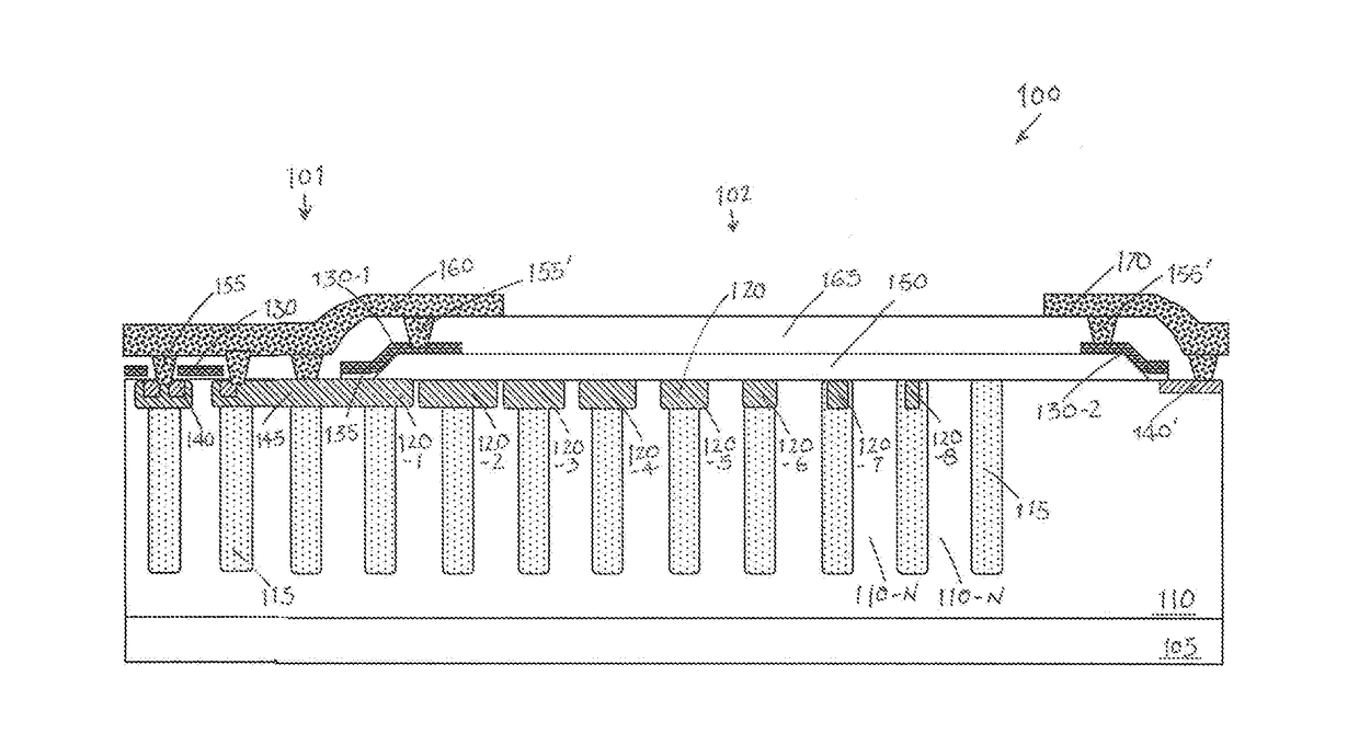
[0016]FIG. 2 is a cross section view of a semiconductor power device 100 as a preferred embodiment of this invention. The semiconductor power device 100 includes an active cell area 101 and a termination area 102 and is formed on an N-type semiconductor substrate 105 supporting an N-type epitaxial layer 110 on top of the bottom substrate layer 105. The epitaxial layer 110 is formed with a super junction structure with the epitaxial layer 110 comprises a plurality of P-columns 115 separated by the 110-N regions between two adjacent P-columns 115. In order to improve the device reliability and the UIS capability, this invention implements a new and improved termination configuration by implanting a plurality of guard rings 120 near the top surface of the epitaxial layer. With the guard rings immediately below the top surface, the surface electric-field can be controlled to distributed over the termination area 102. The device reliability and the UIS capability is improved. As shown in...


PUM


Abstract

This invention discloses a semiconductor power device formed on an upper epitaxial layer of a first conductivity type supported on a semiconductor substrate comprises an active cell area and a termination area disposed near edges of the semiconductor substrate. The semiconductor power device having a super junction structure with the epitaxial layer formed with a plurality of doped columns of a second conductivity type. The termination area further comprises a plurality of surface guard ring regions of the second conductivity type dispose near a top surface of the epitaxial layer close to the doped columns of the second conductivity type. In one of the embodiments, one of the surface guard ring regions extending laterally over several of the doped columns in the termination area.

Description

FIELD OF THE INVENTION[0001]The invention relates generally to semiconductor power devices. More particularly, this invention relates to new configurations and methods for manufacturing improved power device with new edge termination configurations that implement super junction structures with surface guard rings to improve the device reliability and the unclamped inductive switching (UIS) capability.2. DESCRIPTION OF THE RELATED ART[0002]Conventional technologies to configure and manufacture semiconductor power devices operating at the higher voltage are still confronted with difficulties and limitations. Particularly, the configurations and designs of the termination area of a device implemented with super junction structures are critical due to the limitation of crowding of electrical fields that can often leads to device vulnerability and causes unreliable device operations. For these reasons, the configurations and designs of termination are critically important especially for ...

Claims


Application Information

Patent Timeline
IPC IPC(8): H01L29/06H01L29/66H01L29/40H01L21/304H01L21/266H01L21/761H01L21/308H01L21/3065H01L29/78H01L29/10
CPCH01L29/0623H01L29/402H01L29/0634H01L29/1083H01L29/7811H01L29/66712H01L21/308H01L21/304H01L21/266H01L21/761H01L21/3065H01L29/404H01L29/0615H01L29/0619H01L29/0638
Inventor HU, JUN
Owner HUNTECK SEMICON (SHANGHAI) LTD
Why Eureka
Try Eureka