Edge termination designs for semiconductor power devices

a technology of semiconductor power devices and termination designs, which is applied in the direction of semiconductor power devices, basic electric elements, electrical equipment, etc., can solve the problems of unreliable device operation, device configurations as shown may have reliability concerns, and the conventional technology of constructing and manufacturing semiconductor power devices operating at higher voltages are still confronted with difficulties and limitations, and achieves improved termination structure, improved reliability, and improved service life.

Active Publication Date: 2019-07-04
HUNTECH SEMICON SHANGHAI CO LTD
View PDF2 Cites 3 Cited by
  • Summary
  • Abstract
  • Description
  • Claims
  • Application Information

AI Technical Summary

Benefits of technology

[0007]It is an aspect of the present invention to provide a new and improved device configuration and manufacturing method for providing a semiconductor power device with improved termination structure with higher breakdown voltage than the core cell in the active area to achieve good unclamped inductive switch (UIS) capability, improved robust and better device reliability.

Problems solved by technology

Conventional technologies to configure and manufacture semiconductor power devices operating at the higher voltage are still confronted with difficulties and limitations.
Particularly, the configuration and designs of the termination area are critical due to the limitation of breakdown voltage and crowding of electrical fields that can often leads to device vulnerability and causes unreliable device operations.
However, the device configurations as shown may have reliability concerns.
Specifically, the polysilicon in the trenches of FIG. 2B is floating and that may suffer unstable breakdown voltage and leads to poor device reliability.

Method used


Image

  • Edge termination designs for semiconductor power devices
  • Edge termination designs for semiconductor power devices
  • Edge termination designs for semiconductor power devices

Examples


Embodiment Construction

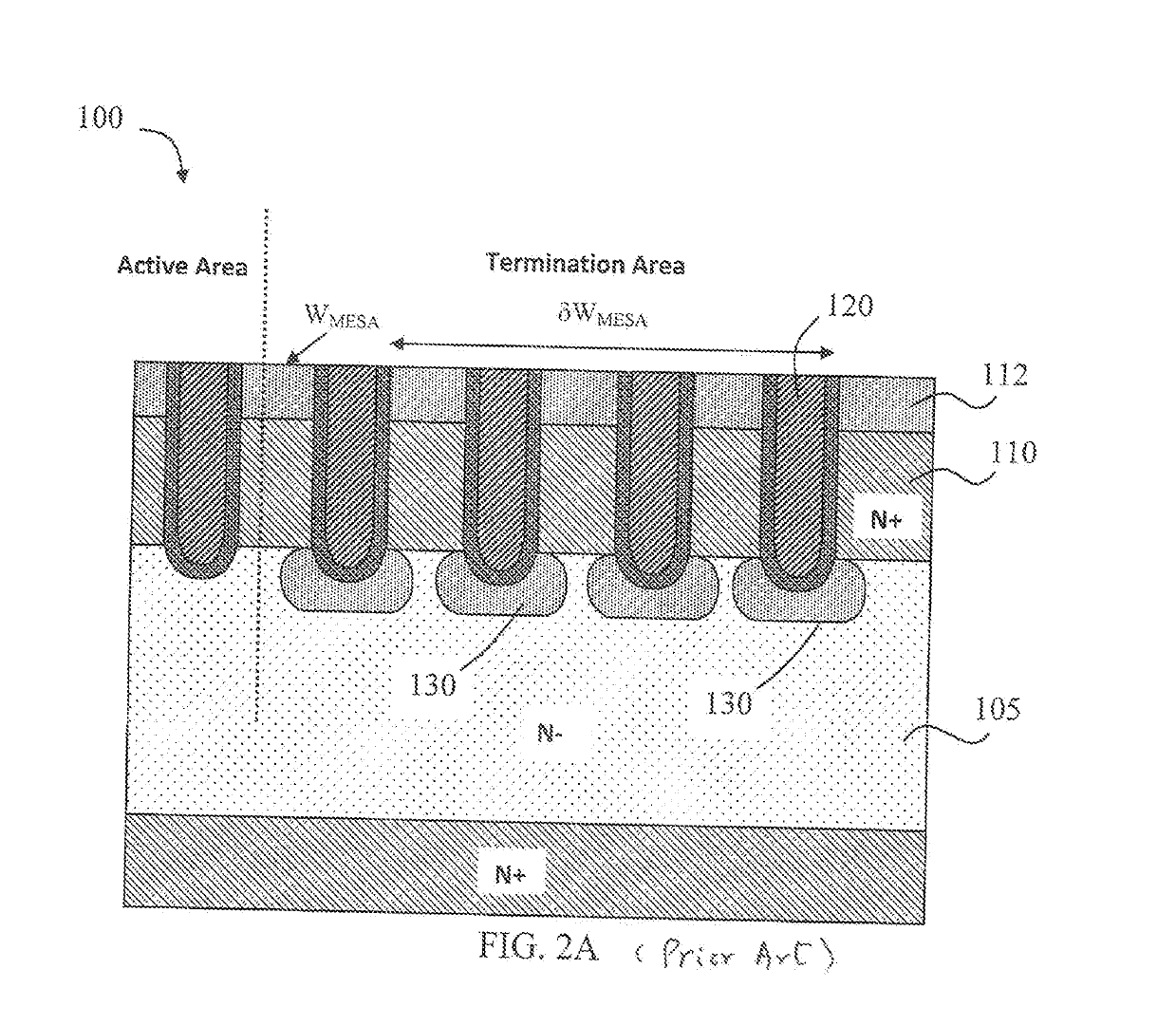
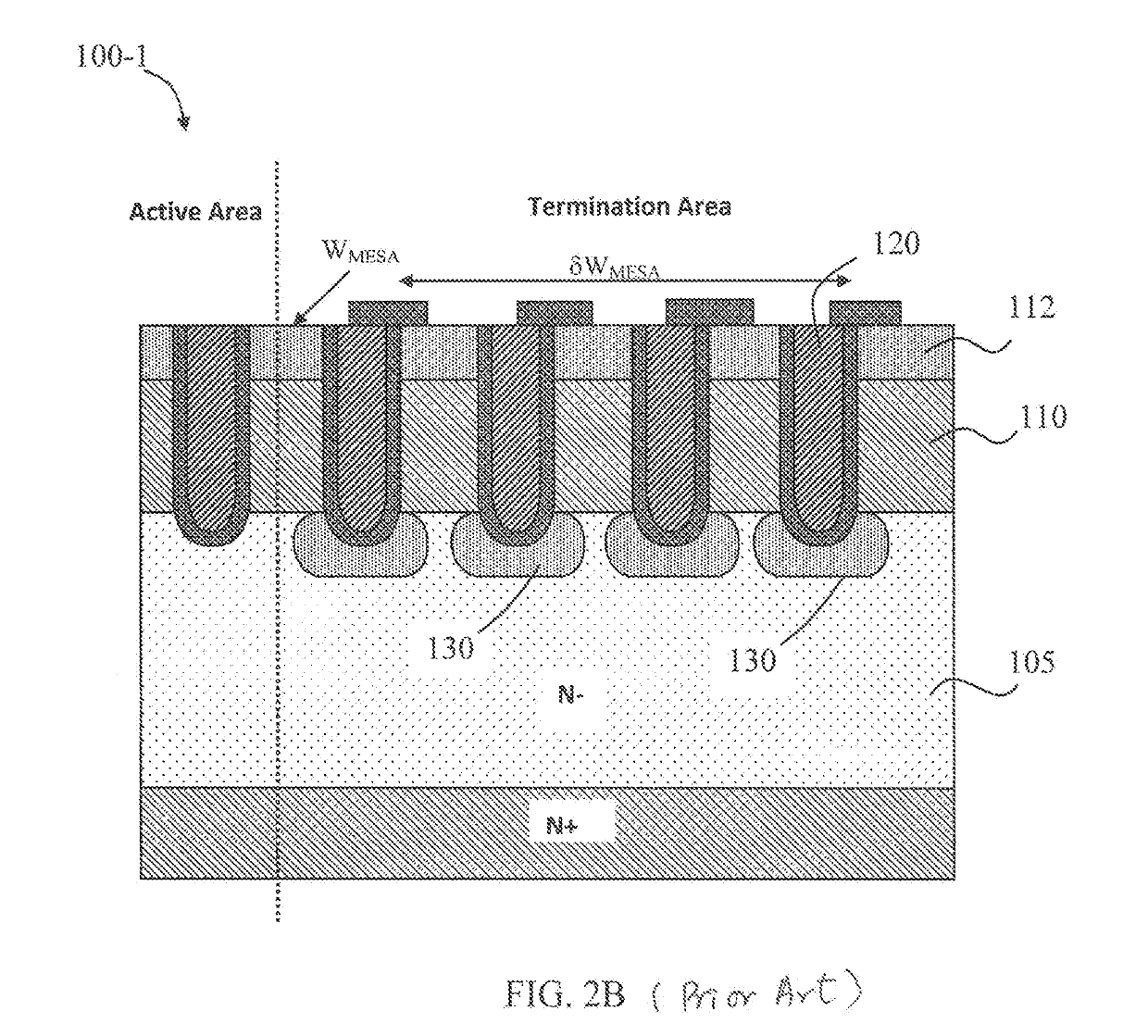
[0023]FIG. 3A is a cross section view of a semiconductor power device 100 as a preferred embodiment of this invention. The semiconductor power device 100 includes an active cell area 101 and a termination area 102 and is formed on an N-type semiconductor substrate 105 supporting an N-type epitaxial layer 110 on top of the bottom substrate layer 105. The active cell area 101 comprises a plurality of transistor cells. Each cell includes a trench 120 with polysilicon filling the trenches having sidewall padded with a shield oxide layer 125. Each transistor cell further includes a P-type body region 135 surrounding the trench 120 near the top surface of the N-type epitaxial layer 110. An insulation layer 140 covers over the top surface. The trench contacts 160 penetrate through the insulation layer to contact the P-type body region 135 and the trench 120 to a source metal layer 150 formed and patterned on top of the insulation layer 140.

[0024]As shown in FIG. 3A, the termination area 10...


PUM


Abstract

This invention discloses a semiconductor power device formed on a semiconductor substrate comprises an active cell area and a termination area disposed near edges of the semiconductor substrate. The termination area comprises a plurality of duplicated units wherein each unit includes at least two trenches filled with a conductive trench material having a mesa area between adjacent trenches wherein the trenches and the mesa areas within each of the duplicated units are electrically shunt together. In the termination area each of the trenches in the duplicated units has a buried guard ring dopant region disposed below a bottom surface of the trenches.

Description

FIELD OF THE INVENTION[0001]The invention relates generally to semiconductor power devices. More particularly, this invention relates to new configurations and methods for manufacturing improved power device with new edge termination structures implemented with trenches and buried guard rings wherein the termination area comprises multiple duplicated units each including two or more than two trenches electrically linked together with the mesa area by metal pad and trench contacts.2. DESCRIPTION OF THE RELATED ART[0002]Conventional technologies to configure and manufacture semiconductor power devices operating at the higher voltage are still confronted with difficulties and limitations. Particularly, the configuration and designs of the termination area are critical due to the limitation of breakdown voltage and crowding of electrical fields that can often leads to device vulnerability and causes unreliable device operations. For these reasons, the configurations and designs of termi...

Claims


Application Information

Patent Timeline
Patent Type & Authority Applications(United States)
IPC IPC(8): H01L29/06H01L21/266H01L21/761
CPCH01L29/0623H01L21/266H01L29/7811H01L29/7823H01L21/761H01L21/2253H01L29/66734H01L29/7813H01L29/404H01L29/407H01L29/0619H01L29/7397H01L29/8613H01L29/66348
Inventor HU, JUNLUO, ZHIYUNWANG, FEI
Owner HUNTECH SEMICON SHANGHAI CO LTD
Why Eureka
Try Eureka