Supercharge Your Innovation With Domain-Expert AI Agents!

Quantum dot ensemble and manufacturing method thereof

a manufacturing method and quantum dot technology, applied in the field of quantum dot ensembles, can solve the problems of significant reduction in yield, difficulty in manufacturing quantum dots having an emission spectrum of a narrow band, and insufficient control of the size and composition of the ensemble,

Inactive Publication Date: 2018-01-25
STANLEY ELECTRIC CO LTD
View PDF1 Cites 5 Cited by
  • Summary
  • Abstract
  • Description
  • Claims
  • Application Information

AI Technical Summary

Problems solved by technology

However, in a case of a ternary mixed crystal, it cannot be said that ease of control of the size and composition thereof is sufficient.
Particularly, in a ternary mixed crystal, an emission spectrum spreads due to variations in the size and composition, and thus, it is difficult to manufacture quantum dots having an emission spectrum of a narrow band.
In addition, after manufacturing the quantum dots, separating and selecting the quantum dots having the variations in the size and composition lead to significant reduction in yield and significant increase in cost, which is not realistic.
However, in the quantum dots which are synthesized through the above methods, it is difficult to control the size and composition, and thus, quantum dots having different size and composition may be mixed into the synthesized quantum dot ensemble.
For this reason, a half-width of an emission spectrum of the quantum dot ensemble broadly spreads in a range of 50 nm to 200 nm, and thus, it is difficult to realize a narrow emission spectrum.
The light emitting wavelength is widened, and thus, it is very difficult to suppress the half width of the emission spectrum to be less than 50 nm.
Meanwhile, also in a core / shell type quantum dots, for example, when a shell layer is formed of a mixed crystal consisting of three or more elements, it is difficult to control a mixed crystal ratio.
That is, the wavelength spectrum of the quantum dot ensemble broadly spreads, and thus, it is difficult to obtain a narrow emission spectrum.

Method used


Image

  • Quantum dot ensemble and manufacturing method thereof
  • Quantum dot ensemble and manufacturing method thereof
  • Quantum dot ensemble and manufacturing method thereof

Examples


first embodiment

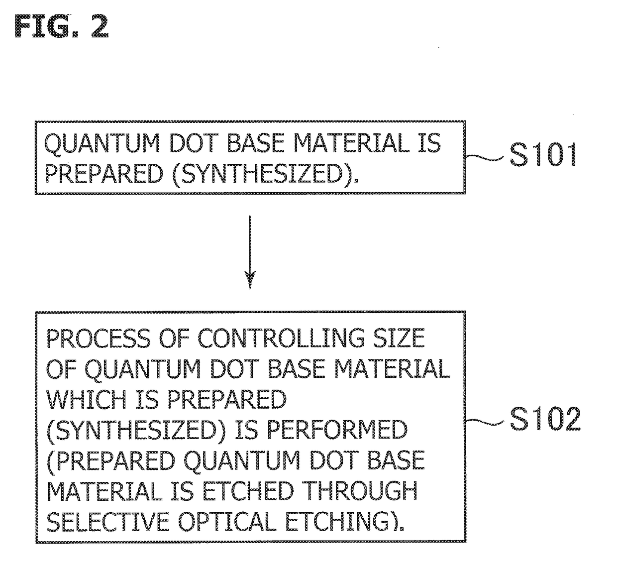
[0042]FIG. 2 is a flow chart schematically illustrating the manufacturing method of the quantum dot ensemble according to the

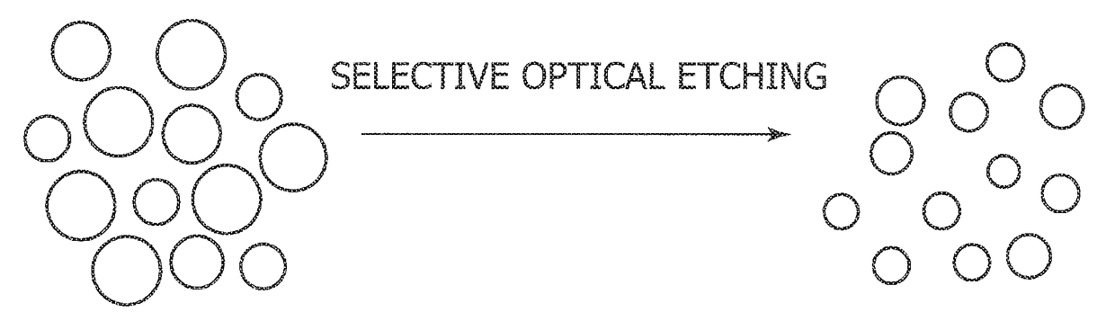
[0043]In the first embodiment, first, a quantum dot base material is prepared, and is synthesized as an example (Step S101). Next, a step of controlling the size of the quantum dot base material which is prepared (synthesized) in Step S101 is performed. Specifically, the prepared quantum dot base material is etched through the selective optical etching (Step S102).

[0044]In a particulating process in the selective optical etching step (Step S102), for example, the quantum dots (the base material) are dispersed in the solution, the dispersion liquid is irradiated with narrow band light. With this, only the particles having the large size are activated by absorbing the light, and then are etched. The quantum dots having the size which is sufficient for absorbing the light aer etched, and thus the size thereof is reduced. When the size is reduced, the band gap bec...

second embodiment

[0076]FIG. 6A is a flow chart schematically illustrating the manufacturing method of the quantum dot ensemble according to the

[0077]In the second embodiment, first, the InyAl1-yN core layer is formed (Step S201a). Next, the ZnOxS1-x shell layer is formed so as to be stacked on the InyAl1-yN core layer formed in Step S201a (Step S201b). Then, the ZnOxS1-x shell layer is etched through the selective optical etching (Step S202).

[0078]Step S201a and Step S201b in the second embodiment are steps corresponding to Step S101 in the first embodiment. In addition, Step S202 in the second embodiment is a step corresponding to Step S102 in the first embodiment.

[0079]In Step S201a, the InyAl1-yN core layer is synthesized by using a liquid phase method such as the hot soap method. In Step S201b, the ZnOxS1-x shell layer including the InyAl1-yN core layer is formed in a size larger than the final target size (thickness). For example, the ZnOxS1-x shell layer is formed in a size (thickness) which i...

third embodiment

[0090]The emission spectrum of the toluene solution in which ZnO0.60S0.40 / AlN nanoparticles which are manufactured through the manufacturing method are dispersed is evaluated with a spectrophotometer. The emission spectrum is observed by using the excitation wavelength of 365 nm, and the emission spectrum having the half width of 45 nm is obtained.

[0091]The quantum dot ensemble (ZnO0.60S0.40 / AlN nanoparticle ensemble) manufactured through the manufacturing method according to the third embodiment exhibits the same effect as that of the quantum dot ensemble manufactured through the manufacturing method according to the second embodiment, for example.

[0092]Note that, the shell layer is formed of the AlN in the third embodiment; however, it is not limited to the AlN. For example, an InwAl1-wN (0wAl1-wN (0

[0093]FIG. 9 is a flow chart schematically illustrating the manufacturing method of the quantum dot ensemble according to the fourt...


PUM

PropertyMeasurementUnit
particle sizeaaaaaaaaaa
sizesaaaaaaaaaa
half-widthaaaaaaaaaa

Abstract

A manufacturing method of a quantum dot ensemble including quantum dots each having a composition represented by a formula AxB1-xCyD1-y (0≦x≦1, 0≦y≦1, A and B are elements selected from Zn and Mg, and C and D are elements selected from the group consisting of O, S, Se, and Te). The quantum dots forming the ensemble in a mixed manner, including (a) step of preparing a plurality of quantum dots each having a composition represented by a formula AxB1-xCyD1-y (0≦x≦1, 0≦y≦1, A and B are elements selected from the group consisting of Zn and Mg, and C and D are elements selected from the group consisting of O, S, Se, and Te); and (b) step of uniformizing band gap energy of the plurality of quantum dots by optically etching the plurality of quantum dots which are prepared in the step (a). In the step (a), target values of x and y in the formula AxB1-xCyD1-y are set in such a manner that band gap energy of AxB1-xCyD1-y attains an approximately minimal value. In the step (b), the quantum dot ensemble including the quantum dots in which at least one of x and y in the formula AxB1-xCyD1-y is varied by equal to or greater than 0.05 is processed, the quantum dot ensemble having an emission spectrum of which the half-width is less than 50 nm is processed, the quantum dot ensemble having a band gap energy which is greater than a band gap energy of a bulk mixed crystal having a same composition as the composition of each of the plurality of quantum dots included in the quantum dot ensemble is processed, and the plurality of quantum dots are processed such that the average particle size thereof is equal to or less than 20 nm.

Description

CROSS-REFERENCE TO RELATED APPLICATION[0001]This application is a Divisional application of U.S. Ser. No. 15 / 005,343, filed on Jan. 25, 2016, which is based upon and claims the benefit of priority of the prior Japanese Patent Applications No. JP 2015-014921, filed on Jan. 29, 2015, and No. JP 2015-248147, filed on Dec. 21, 2015, the entire contents of all of which are incorporated herein by reference.BACKGROUND OF THE INVENTIONA) Field of the Invention[0002]The present invention relates to a quantum dot ensemble, and a manufacturing method thereof. For example, the invention relates to a quantum dot ensemble having a uniform band gap, even when variations in a size and a composition are large, and a manufacturing method thereof. In a case of quantum dots which are formed of a group II-VI ZnOS semiconductor material consisting of ternary or more compositions, a specific effect is exhibited.[0003]The quantum dots are formed by using a semiconductor material and are particles of which ...

Claims


Application Information

Patent Timeline
Patent Type & Authority Applications(United States)
IPC IPC(8): H01L33/50C09K11/02C09K11/08C09K11/62C09K11/64C09K11/56B82Y20/00B82Y30/00B82Y40/00
CPCC09K11/64B82Y40/00C09K11/565C09K11/0883C09K11/02B82Y30/00H01L33/502H01L2933/0041Y10S977/95Y10S977/774Y10S977/824Y10S977/889B82Y20/00H01L2933/0083C09K11/62
Inventor KAZAMA, TAKUYAMIYAKE, YASUYUKITAMURA, WATARU
Owner STANLEY ELECTRIC CO LTD
Features
  • R&D
  • Intellectual Property
  • Life Sciences
  • Materials
  • Tech Scout
  • Unparalleled Data Quality
  • Higher Quality Content
  • 60% Fewer Hallucinations
Learn More